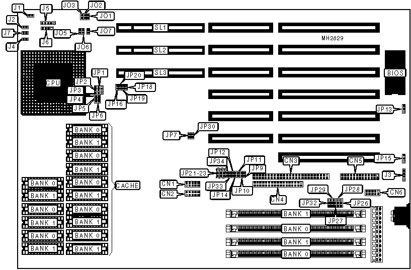
ADVANCED INTEGRATION RESEARCH, INC.
586MI REV. 1.1/1.11/1.12
|
Processor |
Pentium Overdrive/Pentium |
|
Processor Speed |
50/60/66MHz |
|
Chip Set |
Unidentified |
|
Max. Onboard DRAM |
128MB |
|
Cache |
64/128/256/512KB |
|
BIOS |
AMI |
|
Dimensions |
330mm x 218mm |
|
I/O Options |
32-bit VESA local bus slots (3), floppy drive interface, green PC connector, IDE interface, parallel port, serial ports (2) |
|
NPU Options |
None |
|
CONNECTIONS | |||
|
Purpose |
Location |
Purpose |
Location |
|
Serial port 2 |
CN1 |
Turbo LED |
J2 |
|
Serial port 1 |
CN2 |
External battery |
J3 |
|
IDE interface |
CN3 |
IDE interface LED |
J4 |
|
Floppy drive interface |
CN4 |
Power LED & keylock |
J5 |
|
Parallel port |
CN5 |
Speaker |
J6 |
|
Green PC connector |
CN6 |
Turbo switch |
J7 |
|
Reset switch |
J1 |
32-bit VESA local bus slots |
SL1 - SL3 |
|
USER CONFIGURABLE SETTINGS | |||
|
Function |
Jumper |
Position | |
|
» |
Factory configured - do not alter |
JP7 |
N/A |
|
» |
Factory configured - do not alter |
JP9 |
N/A |
|
» |
Factory configured - do not alter |
JP10 |
N/A |
|
» |
Factory configured - do not alter |
JP11 |
N/A |
|
» |
Factory configured - do not alter |
JP12 |
N/A |
|
» |
Flash BIOS programming mode select normal operation |
JP13 |
Open |
|
Flash BIOS programming mode select programming mode |
JP13 |
pins 2 & 3 closed | |
|
» |
Monitor type select monochrome/EGA/VGA |
JP14 |
Open |
|
Monitor type select CGA |
JP14 |
Closed | |
|
» |
CMOS memory normal operation |
JP15 |
pins 2 & 3 closed |
|
CMOS memory clear |
JP15 |
pins 1 & 2 closed | |
|
» |
Factory configured - do not alter |
JP16 |
N/A |
|
» |
Factory configured - do not alter |
JP20 |
N/A |
|
» |
Factory configured - do not alter |
JP26 |
N/A |
|
» |
Factory configured - do not alter |
JP27 |
N/A |
|
» |
Factory configured - do not alter |
JP28 |
N/A |
|
» |
Factory configured - do not alter |
JP29 |
N/A |
|
» |
VL-BUS IDE interface enabled |
JP30 |
Open |
|
VL-BUS IDE interface enabled |
JP30 |
Closed | |
|
» |
Parallel port IRQ select IRQ7 |
JP32 |
pins 1 & 2 closed |
|
Parallel port IRQ select IRQ5 |
JP32 |
pins 2 & 3 closed | |
|
» |
Factory configured - do not alter |
JP33 |
N/A |
|
» |
Factory configured - do not alter |
JP34 |
N/A |
|
DRAM CONFIGURATION | ||
|
Size |
Bank 0 |
Bank 1 |
|
2MB |
(2) 256K x 36 |
NONE |
|
4MB |
(2) 256K x 36 |
(2) 256K x 36 |
|
4MB |
(2) 512K x 36 |
NONE |
|
6MB |
(2) 256K x 36 |
(2) 512K x 36 |
|
8MB |
(2) 512K x 36 |
(2) 512K x 36 |
|
8MB |
(2) 1M x 36 |
NONE |
|
10MB |
(2) 256K x 36 |
(2) 1M x 36 |
|
12MB |
(2) 512K x 36 |
(2) 1M x 36 |
|
16MB |
(2) 1M x 36 |
(2) 1M x 36 |
|
16MB |
(2) 2M x 36 |
NONE |
|
18MB |
(2) 256K x 36 |
(2) 2M x 36 |
|
20MB |
(2) 512K x 36 |
(2) 2M x 36 |
|
24MB |
(2) 1M x 36 |
(2) 2M x 36 |
|
32MB |
(2) 2M x 36 |
(2) 2M x 36 |
|
32MB |
(2) 4M x 36 |
NONE |
|
34MB |
(2) 256K x 36 |
(2) 4M x 36 |
|
40MB |
(2) 1M x 36 |
(2) 4M x 36 |
|
DRAM CONFIGURATION | ||
|
Size |
Bank 0 |
Bank 1 |
|
48MB |
(2) 2M x 36 |
(2) 4M x 36 |
|
64MB |
(2) 4M x 36 |
(2) 4M x 36 |
|
64MB |
(2) 8M x 36 |
NONE |
|
66MB |
(2) 256K x 36 |
(2) 8M x 36 |
|
68MB |
(2) 512K x 36 |
(2) 8M x 36 |
|
72MB |
(2) 1M x 36 |
(2) 8M x 36 |
|
80MB |
(2) 2M x 36 |
(2) 8M x 36 |
|
96MB |
(2) 4M x 36 |
(2) 8M x 36 |
|
128MB |
(2) 8M x 36 |
(2) 8M x 36 |
|
CACHE CONFIGURATION | ||
|
Size |
Bank 0 |
Bank 1 |
|
64KB |
(8) 8K x 8 |
NONE |
|
128KB |
(8) 8K x 8 |
(8) 8K x 8 |
|
256KB |
(8) 32K x 8 |
NONE |
|
512KB |
(8) 32K x 8 |
(8) 32K x 8 |
|
CACHE JUMPER CONFIGURATION | ||||||
|
Size |
JP1 |
JP2 |
JP3 |
JP4 |
JP5 |
JP6 |
|
64KB |
1 & 2 |
1 & 2 |
1 & 2 |
Open |
Open |
Open |
|
128KB |
2 & 3 |
2 & 3 |
2 & 3 |
Open |
Open |
Closed |
|
256KB |
1 & 2 |
1 & 2 |
1 & 2 |
Open |
Closed |
Closed |
|
512KB |
2 & 3 |
2 & 3 |
2 & 3 |
Closed |
Closed |
Closed |
|
Note: Pins designated should be in the closed position. | ||||||
|
CPU SPEED CONFIGURATION | |||
|
Speed |
JO1 |
JO2 |
JO3 |
|
50MHz |
Open |
Open |
Closed |
|
60MHz |
Open |
Closed |
Open |
|
66MHz |
Closed |
Closed |
Open |
|
VESA WAIT STATE CONFIGURATION | |
|
Wait states |
JP18 |
|
0 wait states |
Open |
|
1 wait state |
Closed |
|
BUS SPEED CONFIGURATION | ||||
|
CPU speed |
JO5 |
JO6 |
JO7 |
JP19 |
|
<= 33MHz |
Closed |
Open |
Open |
Open |
|
> 33MHz |
Open |
Open |
Open |
Closed |
|
IDE RECOVERY TIME CONFIGURATION | |||
|
Speed |
JP21 |
JP22 |
JP23 |
|
0 |
pins 2 & 3 closed |
pins 2 & 3 closed |
pins 2 & 3 closed |
|
1 |
pins 1 & 2 closed |
pins 2 & 3 closed |
pins 2 & 3 closed |
|
2 |
pins 2 & 3 closed |
pins 1 & 2 closed |
pins 2 & 3 closed |