ACER, INC.
V12P
|
Processor |
Pentium |
|
Processor Speed |
Unidentified |
|
Chip Set |
Unidentified |
|
Video Chip Set |
None |
|
Maximum Onboard Memory |
192MB |
|
Maximum Video Memory |
None |
|
Cache |
256/512KB |
|
BIOS |
Unidentified |
|
Dimensions |
330mm x 218mm |
|
I/O Options |
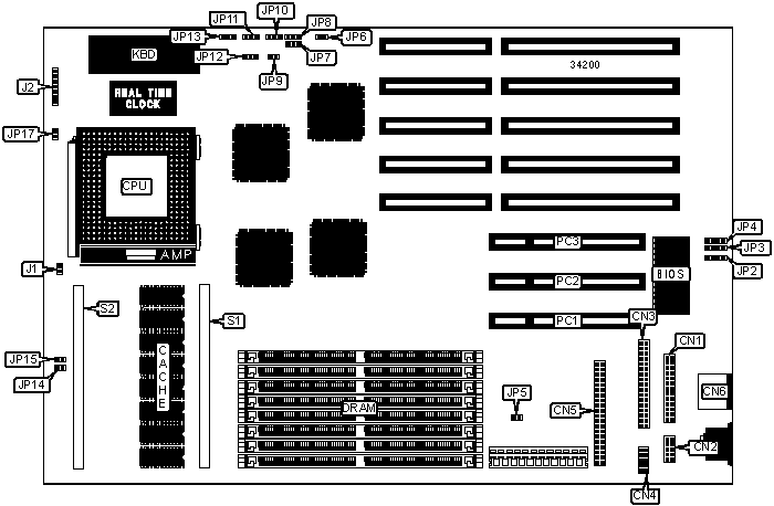
32-bit PCI slots (3), floppy drive interface, IDE interface, parallel port, PS/2 mouse port, serial ports (2) |
|
NPU Options |
None |
|
CONNECTIONS | |||
|
Purpose |
Location |
Purpose |
Location |
|
Parallel port |
CN1 |
IDE interface |
CN5 |
|
Serial port 2 |
CN2 |
Chassis fan power |
J1 |
|
Floppy drive interface |
CN3 |
Keyboard & PS/2 mouse connector |
J2 |
|
Serial port 1 |
CN4 |
32-bit PCI slots |
PC1 - PC3 |
|
USER CONFIGURABLE SETTINGS | |||
|
Function |
Label |
Position | |
|
MS105 SIO chip enabled |
JP5 |
Closed | |
|
MS105 SIO chip disabled |
JP5 |
Open | |
|
Parallel port bidirectional |
JP6 |
Closed | |
|
Parallel port unidirectional |
JP6 |
Open | |
|
» |
Factory configured - do not alter |
JP7 |
Unidentified |
|
» |
Factory configured - do not alter |
JP8 |
Unidentified |
|
» |
Factory configured - do not alter |
JP9 |
Unidentified |
|
Password disabled |
JP11 |
Pins 1 & 2 closed | |
|
Password enabled |
JP11 |
Pins 2 & 3 closed | |
|
Keylock disabled |
JP17 |
Closed | |
|
Keylock enabled |
JP17 |
Open | |
|
DRAM CONFIGURATION | |||
|
Size |
Bank 0 |
Bank 1 |
Bank 2 |
|
4MB |
(2) 1M x 36 |
None |
None |
|
8MB |
(2) 1M x 36 |
(2) 1M x 36 |
None |
|
16MB |
(2) 1M x 36 |
(2) 1M x 36 |
None |
|
16MB |
(2) 2M x 36 |
None |
None |
|
24MB |
(2) 2M x 36 |
(2) 1M x 36 |
None |
|
24MB |
(2) 1M x 36 |
(2) 1M x 36 |
(2) 1M x 36 |
|
32MB |
(2) 4M x 36 |
None |
None |
|
32MB |
(2) 2M x 36 |
(2) 2M x 36 |
None |
|
40MB |
(2) 4M x 36 |
(2) 1M x 36 |
None |
|
48MB |
(2) 4M x 36 |
(2) 2M x 36 |
None |
|
48MB |
(2) 4M x 36 |
(2) 1M x 36 |
(2) 1M x 36 |
|
56MB |
(2) 4M x 36 |
(2) 2M x 36 |
(2) 1M x 36 |
|
64MB |
(2) 8M x 36 |
None |
None |
|
64MB |
(2) 4M x 36 |
(2) 4M x 36 |
None |
|
80MB |
(2) 8M x 36 |
(2) 2M x 36 |
None |
|
80MB |
(2) 8M x 36 |
(2) 1M x 36 |
(2) 1M x 36 |
|
88MB |
(2) 8M x 36 |
(2) 2M x 36 |
(2) 1M x 36 |
|
96MB |
(2) 8M x 36 |
(2) 4M x 36 |
None |
|
96MB |
(2) 4M x 36 |
(2) 4M x 36 |
(2) 4M x 36 |
|
96MB |
(2) 8M x 36 |
(2) 2M x 36 |
(2) 2M x 36 |
|
104MB |
(2) 8M x 36 |
(2) 4M x 36 |
(2) 1M x 36 |
|
112MB |
(2) 8M x 36 |
(2) 4M x 36 |
(2) 2M x 36 |
|
128MB |
(2) 8M x 36 |
(2) 4M x 36 |
(2) 4M x 36 |
|
128MB |
(2) 16M x 36 |
None |
None |
|
128MB |
(2) 8M x 36 |
(2) 8M x 36 |
None |
|
DRAM CONFIGURATION (CON'T) | |||
|
Size |
Bank 0 |
Bank 1 |
Bank 2 |
|
136MB |
(2) 8M x 36 |
(2) 8M x 36 |
(2) 1M x 36 |
|
136MB |
(2) 16M x 36 |
(2) 1M x 36 |
None |
|
144MB |
(2) 16M x 36 |
(2) 2M x 36 |
None |
|
144MB |
(2) 16M x 36 |
(2) 1M x 36 |
(2) 1M x 36 |
|
160MB |
(2) 16M x 36 |
(2) 4M x 36 |
None |
|
160MB |
(2) 16M x 36 |
(2) 2M x 36 |
(2) 2M x 36 |
|
192MB |
(2) 16M x 36 |
(2) 8M x 36 |
None |
|
192MB |
(2) 16M x 36 |
(2) 4M x 36 |
(2) 4M x 36 |
|
Note: The location of the banks is unidentified. | |||
|
CACHE CONFIGURATION |
|
Note: Board accepts 256KB/512KB cache. 256KB is factory installed and is not configurable. To upgrade to 512KB, install cache module at S1/S2. The size and actual configuration of the module is unidentified. |
|
CACHE JUMPER CONFIGURATION | ||
|
Size |
JP10 |
JP12 |
|
None |
Pins 1 & 2 closed |
Pins 1 & 2 closed |
|
256KB |
Pins 2 & 3 closed |
Pins 1 & 2 closed |
|
512KB |
Pins 2 & 3 closed |
Pins 2 & 3 closed |
|
CACHE SIGNAL CONFIGURATION | ||
|
Setting |
JP14 |
JP15 |
|
Enabled |
Closed |
Closed |
|
Disabled |
Open |
Open |
|
CACHE TYPE CONFIGURATION | |
|
Type |
JP13 |
|
Standard |
Pins 1 & 2 closed |
|
Burst |
Pins 2 & 3 closed |
|
PCI INTERRUPT B SELECTION | |
|
Setting |
JP2 |
|
IRQ14 |
Pins 3 & 4 closed |
|
IRQ15 |
Pins 1 & 2 closed |
|
Disabled |
Pins 2 & 3 closed |
|
PCI INTERRUPT C SELECTION | |
|
Setting |
JP3 |
|
IRQ11 |
Pins 1 & 2 closed |
|
IRQ15 |
Pins 2 & 3 closed |
|
Disabled |
Pins 3 & 4 closed |
|
PCI INTERRUPT D SELECTION | |
|
Setting |
JP4 |
|
IRQ10 |
Pins 1 & 2 closed |
|
IRQ15 |
Pins 3 & 4 closed |
|
Disabled |
Pins 2 & 3 closed |