ACER, INC.
AP55CS
|
Device Type |
Mainboard |
|
Processor |
CX 6X86/Pentium |
|
Processor Speed |
75/90/100/120/133/150/166MHz |
|
Chip Set |
SIS |
|
Video Chip Set |
Unidentified |
|
Maximum Onboard Memory |
128MB (EDO supported) Unified Memory Architecture (UMA) |
|
Cache |
256KB |
|
BIOS |
AMI |
|
Dimensions |
280mm x 220mm |
|
I/O Options |
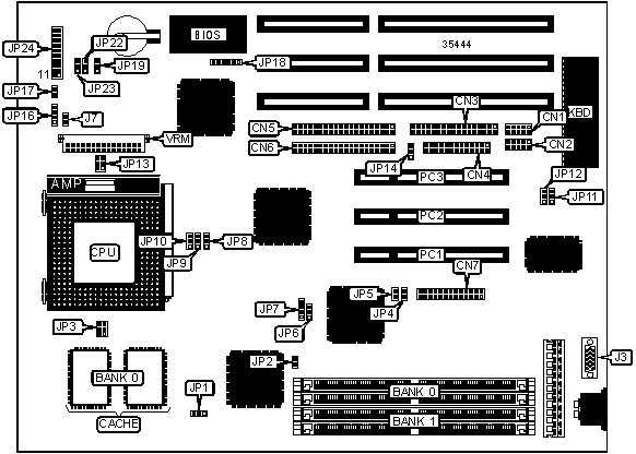
32-bit PCI slots (3), floppy drive interface, IDE interfaces (2), parallel port, serial ports (2), VGA feature connector, VGA port, VRM connector |
|
NPU Options |
None |
|
CONNECTIONS | |||
|
Purpose |
Location |
Purpose |
Location |
|
Serial port 1 |
CN1 |
IDE interface LED |
JP16 |
|
Serial port 2 |
CN2 |
Power LED & keylock |
JP24/pins 1 – 5 |
|
Floppy drive interface |
CN3 |
Speaker |
JP24/pins 7 – 10 |
|
Parallel port |
CN4 |
Turbo LED |
JP24/pins 12 & 13 |
|
IDE interface 2 |
CN5 |
Turbo switch |
JP24/pins 15 – 17 |
|
IDE interface 1 |
CN6 |
Reset switch |
JP24/pins 19 & 20 |
|
VGA feature connector |
CN7 |
32-bit PCI slots |
PC1 – PC3 |
|
VGA port |
J3 |
VRM connector |
VRM |
|
CPU fan power |
J7 | ||
|
USER CONFIGURABLE SETTINGS | |||
|
Function |
Label |
Position | |
|
» |
Factory configured - do not alter |
JP2 |
Unidentified |
|
» |
Factory configured - do not alter |
JP3 |
Unidentified |
|
» |
Factory configured - do not alter |
JP5 |
Unidentified |
|
» |
Factory configured - do not alter |
JP8 |
Unidentified |
|
» |
Factory configured - do not alter |
JP13 |
Unidentified |
|
On board I/O enabled |
JP14 |
Pins 1 & 2 closed | |
|
On board I/O disabled |
JP14 |
Pins 2 & 3 closed | |
|
» |
Factory configured - do not alter |
JP17 |
Unidentified |
|
» |
CMOS memory normal operation |
JP19 |
Pins 1 & 2 closed |
|
CMOS memory clear |
JP19 |
Pins 2 & 3 closed | |
|
SIMM CONFIGURATION | ||
|
Size |
Bank 0 |
Bank 1 |
|
2MB |
(2) 256K x 36 |
None |
|
4MB |
(2) 512K x 36 |
None |
|
4MB |
(2) 256K x 36 |
(2) 256K x 36 |
|
6MB |
(2) 512K x 36 |
(2) 256K x 36 |
|
8MB |
(2) 512K x 36 |
(2) 512K x 36 |
|
8MB |
(2) 1M x 36 |
None |
|
10MB |
(2) 1M x 36 |
(2) 256K x 36 |
|
12MB |
(2) 1M x 36 |
(2) 512K x 36 |
|
16MB |
(2) 2M x 36 |
None |
|
16MB |
(2) 1M x 36 |
(2) 1M x 36 |
|
18MB |
(2) 2M x 36 |
(2) 256K x 36 |
|
SIMM CONFIGURATION (CON’T) | ||
|
Size |
Bank 0 |
Bank 1 |
|
20MB |
(2) 2M x 36 |
(2) 512K x 36 |
|
24MB |
(2) 2M x 36 |
(2) 1M x 36 |
|
32MB |
(2) 4M x 36 |
None |
|
32MB |
(2) 2M x 36 |
(2) 2M x 36 |
|
34MB |
(2) 4M x 36 |
(2) 256K x 36 |
|
36MB |
(2) 4M x 36 |
(2) 512K x 36 |
|
40MB |
(2) 4M x 36 |
(2) 1M x 36 |
|
48MB |
(2) 4M x 36 |
(2) 2M x 36 |
|
64MB |
(2) 8M x 36 |
None |
|
64MB |
(2) 4M x 36 |
(2) 4M x 36 |
|
66MB |
(2) 8M x 36 |
(2) 256K x 36 |
|
68MB |
(2) 8M x 36 |
(2) 512K x 36 |
|
72MB |
(2) 8M x 36 |
(2) 1M x 36 |
|
80MB |
(2) 8M x 36 |
(2) 2M x 36 |
|
96MB |
(2) 8M x 36 |
(2) 4M x 36 |
|
128MB |
(2) 8M x 36 |
(2) 8M x 36 |
|
Note: Board accepts EDO memory. | ||
|
CACHE CONFIGURATION | |
|
Size |
Bank 0 |
|
256KB |
(2) 32K x 32 |
|
CACHE TYPE CONFIGURATION | |
|
Type |
JP1 |
|
Linear mode |
Pins 1 & 2 closed |
|
Interleave mode |
Pins 2 & 3 closed |
|
CPU SPEED SELECTION (CX 6X86) | ||||||
|
CPU speed |
Clock speed |
Multiplier |
JP9 |
JP10 |
JP22 |
JP23 |
|
120MHz |
50MHz |
2x |
2 & 3 |
2 & 3 |
Open |
Open |
|
150MHz |
60MHz |
2x |
2 & 3 |
1 & 2 |
Open |
Open |
|
166MHz |
66MHz |
2x |
1 & 2 |
2 & 3 |
Open |
Open |
|
Note: Pins designated should be in the closed position. | ||||||
|
CPU SPEED SELECTION (INTEL) | ||||||
|
CPU speed |
Clock speed |
Multiplier |
JP9 |
JP10 |
JP22 |
JP23 |
|
75MHz |
50MHz |
1.5x |
2 & 3 |
2 & 3 |
2 & 3 |
2 & 3 |
|
90MHz |
60MHz |
1.5x |
2 & 3 |
1 & 2 |
2 & 3 |
2 & 3 |
|
100MHz |
66MHz |
1.5x |
1 & 2 |
2 & 3 |
2 & 3 |
2 & 3 |
|
120MHz |
60MHz |
2x |
2 & 3 |
1 & 2 |
1 & 2 |
2 & 3 |
|
133MHz |
66MHz |
2x |
1 & 2 |
2 & 3 |
1 & 2 |
2 & 3 |
|
150MHz |
60MHz |
2.5x |
2 & 3 |
1 & 2 |
1 & 2 |
1 & 2 |
|
166MHz |
66MHz |
2.5x |
1 & 2 |
2 & 3 |
1 & 2 |
1 & 2 |
|
Note: Pins designated should be in the closed position. | ||||||
|
DMA CHANNEL SELECTION | ||
|
Channel |
JP11 |
JP12 |
|
1 |
Pins 2 & 3 closed |
Pins 2 & 3 closed |
|
3 |
Pins 1 & 2 closed |
Pins 1 & 2 closed |
|
ON BOARD VIDEO SELECTION | |||
|
Setting |
JP4 |
JP6 |
JP7 |
|
Enabled |
Closed |
Pins 1 & 2 closed |
Pins 2 & 3 closed |
|
Disabled |
Open |
Pins 2 & 3 closed |
Pins 3 & 4 closed |
|
FLASH BIOS SELECTION | |
|
Setting |
JP18 |
|
5v |
Pins 2 & 3, 5 & 6 closed |
|
12v |
Pins 1 & 2, 5 & 6 closed |
|
EEPROM |
Pins 2 & 3, 4 & 5 closed |