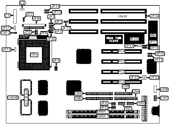
ACER, INC.
AP5V
|
Device Type |
Mainboard |
|
Processor |
Pentium |
|
Processor Speed |
75/90/100/120/133/150/166/200MHz |
|
Chip Set |
Intel 430VX |
|
Video Chip Set |
None |
|
Maximum Onboard Memory |
128MB (EDO & SDRAM supported) |
|
Maximum Video Memory |
None |
|
Cache |
256/512KB |
|
BIOS |
AMI |
|
Dimensions |
280mm x 220mm |
|
I/O Options |
32-bit PCI slots (4), floppy drive interface, IDE interfaces (2), parallel port, PS/2 mouse port, serial ports (2), VRM connector, USB connector |
|
CONNECTIONS | |||
|
Purpose |
Location |
Purpose |
Location |
|
Front panel connector |
C1 |
IDE interface 1 |
CN6 |
|
IDE interface LED |
C2 |
PS/2 mouse interface |
CN7 |
|
Serial port 1 |
CN1 |
Chassis fan power |
CN12 |
|
Serial port 2 |
CN2 |
32-bit PCI slots |
PC1 – PC4 |
|
Parallel port |
CN3 |
USB connector |
USB |
|
Floppy drive interface |
CN4 |
VRM connector |
VRM |
|
IDE interface 2 |
CN5 | ||
|
USER CONFIGURABLE SETTINGS | |||
|
Function |
Label |
Position | |
|
» |
CMOS memory normal operation |
JP12 |
Pins 1 & 2 closed |
|
CMOS memory clear |
JP12 |
Pins 2 & 3 closed | |
|
» |
On board I/O enabled |
JP13 |
Pins 1 & 2 closed |
|
On board I/O disabled |
JP13 |
Pins 2 & 3 closed | |
|
» |
ISA clock select CLK/3 |
JP14 |
Pins 1 & 2 closed |
|
ISA clock select CLK/4 |
JP14 |
Pins 2 & 3 closed | |
|
» |
PS/2 mouse enabled |
JP15 |
Pins 1 & 2 closed |
|
PS/2 mouse disabled |
JP15 |
Pins 2 & 3 closed | |
|
» |
Flash BIOS voltage select 5v |
JP16 |
Pins 2 & 3 closed |
|
Flash BIOS voltage select 12v |
JP16 |
Pins 1 & 2 closed | |
|
» |
Factory configured - do not alter |
JP17 |
Unidentified |
|
» |
Factory configured - do not alter |
JP18 |
Unidentified |
|
» |
Factory configured - do not alter |
JP20 |
Unidentified |
|
» |
Factory configured - do not alter |
JP21 |
Unidentified |
|
» |
Factory configured - do not alter |
JP22 |
Unidentified |
|
» |
Factory configured - do not alter |
JP23 |
Unidentified |
|
» |
Keyboard clock select 8MHz |
JP24 |
Pins 1 & 2 closed |
|
Keyboard clock select 12MHz |
JP24 |
Pins 2 & 3 closed | |
|
DIMM CONFIGURATION | ||
|
Size |
Bank 0 |
Bank 1 |
|
8MB |
(1) 1M x 64 |
None |
|
16MB |
(1) 2M x 64 |
None |
|
16MB |
(1) 1M x 64 |
(1) 1M x 64 |
|
24MB |
(1) 2M x 64 |
(1) 1M x 64 |
|
32MB |
(1) 4M x 64 |
None |
|
32MB |
(1) 2M x 64 |
(1) 2M x 64 |
|
40MB |
(1) 4M x 64 |
(1) 1M x 64 |
|
48MB |
(1) 4M x 64 |
(1) 2M x 64 |
|
64MB |
(1) 8M x 64 |
None |
|
64MB |
(1) 4M x 64 |
(1) 4M x 64 |
|
72MB |
(1) 8M x 64 |
(1) 1M x 64 |
|
80MB |
(1) 8M x 64 |
(1) 2M x 64 |
|
96MB |
(1) 8M x 64 |
(1) 4M x 64 |
|
128MB |
(1) 8M x 64 |
(1) 8M x 64 |
|
Note: Board accepts EDO & SDRAM memory. | ||
|
DIMM CONFIGURATION | |||
|
Type |
JP8 |
JP9 | |
| » |
SDRAM |
Open |
Open |
|
EDO |
Pins 1 & 2, 3 & 4, 5 & 6 closed |
Pins 1 & 2, 3 & 4, 5 & 6 closed | |
|
CACHE CONFIGURATION | |
|
Size |
Bank 0 |
|
256KB |
(2) 32K x 32 |
|
512KB |
(2) 64K x 32 |
|
CPU SPEED SELECTION | ||||||
|
CPU speed |
Clock speed |
Multiplier |
JP1 |
JP2 |
JP3 |
JP4 |
|
75MHz |
50MHz |
1.5x |
1 & 2 |
1 & 2 |
1 & 2 |
1 & 2 |
|
90MHz |
60MHz |
1.5x |
1 & 2 |
1 & 2 |
2 & 3 |
1 & 2 |
|
100MHz |
66MHz |
1.5x |
1 & 2 |
1 & 2 |
1 & 2 |
2 & 3 |
|
120MHz |
60MHz |
2x |
1 & 2 |
2 & 3 |
2 & 3 |
1 & 2 |
|
133MHz |
66MHz |
2x |
1 & 2 |
2 & 3 |
1 & 2 |
2 & 3 |
|
150MHz |
60MHz |
2.5x |
2 & 3 |
2 & 3 |
2 & 3 |
1 & 2 |
|
166MHz |
66MHz |
2.5x |
2 & 3 |
2 & 3 |
1 & 2 |
2 & 3 |
|
200MHz |
66MHz |
3x |
2 & 3 |
1 & 2 |
1 & 2 |
2 & 3 |
|
Note: Pins designated should be in the closed position. | ||||||
|
CPU TYPE SELECTION | |||
|
Type |
JP5 |
JP6 | |
| » |
P54C |
Pins 1 & 2, 3 & 4, 5 & 6 closed |
Pins 1 & 2, 3 & 4, 5 & 6 closed |
|
P55C |
Open |
Open | |
|
CPU VOLTAGE SELECTION | |
|
Voltage |
JP7 |
|
3.45v |
Pins 1 & 2 closed |
|
3.52v |
Pins 2 & 3 closed |
|
DMA CHANNEL SELECTION | |||
|
Channel |
JP10 |
JP11 | |
|
1 |
Pins 2 & 3 closed |
Pins 2 & 3 closed | |
| » |
3 |
Pins 1 & 2 closed |
Pins 1 & 2 closed |