ACER, INC.
V30
|
Device Type |
Mainboard |
|
Processor |
Pentium |
|
Processor Speed |
75/90/100/120/133/150/166MHz |
|
Chip Set |
Unidentified |
|
Maximum Onboard Memory |
128MB (EDO & SDRAM supported) |
|
Cache |
256/512KB |
|
BIOS |
Unidentified |
|
Dimensions |
330mm x 218mm |
|
I/O Options |
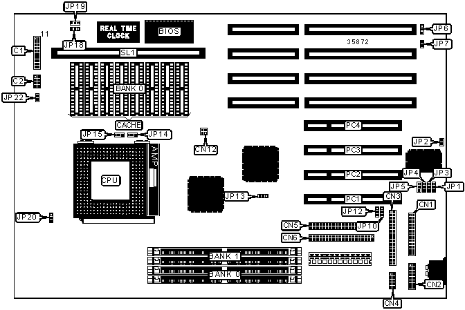
32-bit PCI slots (3), floppy drive interface, green PC connector, IDE interfaces (2), parallel port, PS/2 mouse port, PS/2 mouse interface, serial ports (2), cache slot |
|
CONNECTIONS | |||
|
Purpose |
Location |
Purpose |
Location |
|
Power LED & keylock |
C1/pins 1 – 5 |
Serial port 1 |
CN4 |
|
Speaker |
C1/pins 7 – 10 |
IDE interface 1 |
CN5 |
|
Turbo LED |
C1/pins 12 & 13 |
IDE interface 2 |
CN6 |
|
Turbo switch |
C1/pins 15 – 17 |
External battery |
JP16 |
|
Reset switch |
C1/pins 19 & 20 |
Chassis fan power |
JP21 |
|
ID3P LED |
C2 |
IDE interface LED |
JP23 |
|
Parallel port |
CN1 |
32-bit PCI slots |
PC1 – PC4 |
|
Serial port 2 |
CN2 |
Cache slot |
SL1 |
|
Floppy drive interface |
CN3 | ||
|
Note: The location JP16, JP21 & JP23 are unidentified. | |||
|
USER CONFIGURABLE SETTINGS | |||
|
Function |
Label |
Position | |
|
» |
Factory configured - do not alter |
JP1 |
Open |
|
Standard function enabled |
JP2 |
Open | |
|
ECP function enabled |
JP2 |
Closed | |
|
On board I/O enabled |
JP5 |
Pins 1 & 2 closed | |
|
On board I/O disabled |
JP5 |
Pins 2 & 3 closed | |
|
Password normal operation |
JP6 |
Pins 1 & 2 closed | |
|
Password clear |
JP6 |
Pins 2 & 3 closed | |
|
Keyboard IRQ12 disabled |
JP7 |
Open | |
|
Keyboard IRQ12 enabled |
JP7 |
Closed | |
|
» |
Factory configured - do not alter |
JP10 |
Closed |
|
» |
Factory configured - do not alter |
JP12 |
Closed |
|
» |
CMOS memory normal operation |
JP17 |
Pins 2 & 3 closed |
|
CMOS memory clear |
JP17 |
Pins 1 & 2 closed | |
|
» |
Factory configured - do not alter |
JP18 |
Pins 1 & 2 closed |
|
» |
Factory configured - do not alter |
JP19 |
Open |
|
» |
Factory configured - do not alter |
JP22 |
Closed |
|
Note: The location JP17 is unidentified. | |||
|
SIMM CONFIGURATION | ||
|
Size |
Bank 0 |
Bank 1 |
|
8MB |
(2) 1M x 36 |
None |
|
16MB |
(2) 2M x 36 |
None |
|
16MB |
(2) 1M x 36 |
(2) 1M x 36 |
|
24MB |
(2) 2M x 36 |
(2) 1M x 36 |
|
32MB |
(2) 4M x 36 |
None |
|
32MB |
(2) 2M x 36 |
(2) 2M x 36 |
|
40MB |
(2) 4M x 36 |
(2) 1M x 36 |
|
48MB |
(2) 4M x 36 |
(2) 2M x 36 |
|
64MB |
(2) 8M x 36 |
None |
|
64MB |
(2) 4M x 36 |
(2) 4M x 36 |
|
72MB |
(2) 8M x 36 |
(2) 1M x 36 |
|
80MB |
(2) 8M x 36 |
(2) 2M x 36 |
|
96MB |
(2) 8M x 36 |
(2) 4M x 36 |
|
128MB |
(2) 8M x 36 |
(2) 8M x 36 |
|
Note: Board accepts EDO memory. | ||
|
CACHE CONFIGURATION | ||
|
Size |
Bank 0 |
SL1 |
|
256KB |
(8) 32K x 8 |
Not installed |
|
512KB |
(8) 32K x 8 |
256KB module installed |
|
CPU SPEED SELECTION | ||||||
|
CPU speed |
Clock speed |
Multiplier |
CN12 |
JP13 |
JP14 |
JP15 |
|
75MHz |
50MHz |
1.5x |
1 & 3, 2 & 4 |
1 & 2 |
1 & 2 |
1 & 2 |
|
90MHz |
60MHz |
1.5x |
1 & 3 |
2 & 3 |
1 & 2 |
1 & 2 |
|
100MHz |
66MHz |
1.5x |
2 & 4 |
2 & 3 |
1 & 2 |
1 & 2 |
|
120MHz |
60MHz |
2x |
1 & 3 |
2 & 3 |
1 & 2 |
2 & 3 |
|
133MHz |
66MHz |
2x |
2 & 4 |
2 & 3 |
1 & 2 |
2 & 3 |
|
150MHz |
60MHz |
2.5x |
1 & 3 |
2 & 3 |
2 & 3 |
2 & 3 |
|
166MHz |
66MHz |
2.5x |
2 & 4 |
2 & 3 |
2 & 3 |
2 & 3 |
|
Note: Pins designated should be in the closed position. | ||||||
|
CPU TYPE SELECTION | |
|
Type |
JP20 |
|
VR |
Pins 1 & 2 closed |
|
VRE |
Pins 2 & 3 closed |
|
DMA CHANNEL SELECTION | ||
|
Channel |
JP3 |
JP4 |
|
1 |
Pins 2 & 3 closed |
Pins 1 & 2 closed |
|
3 |
Pins 1 & 2 closed |
Pins 2 & 3 closed |