ACER, INC.
V55LA
|
Device Type |
Mainboard |
|
Processor |
Pentium/CX 6X86/AM K5 |
|
Processor Speed |
75/90/100/120/133/150/166/200MHz |
|
Chip Set |
Unidentified |
|
Video Chip Set |
Unidentified |
|
Maximum Onboard Memory |
128MB (EDO & SDRAM supported) |
|
Maximum Video Memory |
2MB |
|
Cache |
256/512KB |
|
BIOS |
Unidentified |
|
Dimensions |
254mm x 218mm |
|
I/O Options |
Bus mouse port, Ethernet 10BaseT connector, green PC connector, IDE interfaces (2), parallel port, PS/2 mouse port, serial ports (2), VGA port, riser slot, IR connector, line in, wavetable connector, audio in - CD-ROM |
|
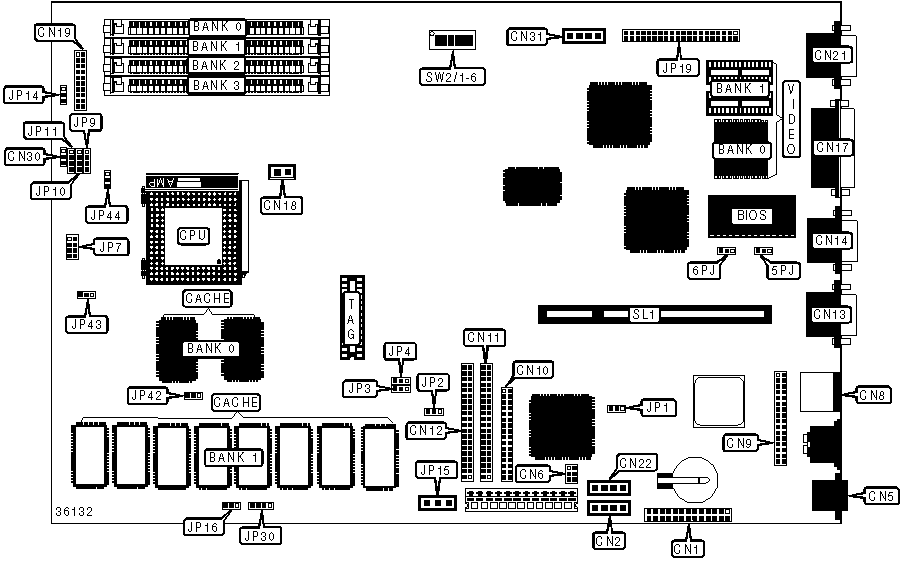
CONNECTIONS | |||
|
Purpose |
Location |
Purpose |
Location |
|
Multimedia/ethernet connector |
CN1 |
Turbo LED |
CN19/pins 12 & 13 |
|
Audio in - CD-ROM |
CN2 |
Turbo |
CN19/pins 15 - 17 |
|
LAN connector |
CN5 |
Reset |
CN19/pins 19 & 20 |
|
Wavetable |
CN6 |
Video port |
CN21 |
|
PS/2 mouse port |
CN8 |
Fax/modem connector |
CN22 |
|
Audio I/O board connector |
CN9 |
Reset switch connector |
CN30 |
|
Floppy drive interface |
CN10 |
Line in |
CN31 |
|
IDE interface 2 |
CN11 |
Power LED & hard disk |
JP9 |
|
IDE interface 1 |
CN12 |
Disk LED |
JP10 |
|
Serial port 1 |
CN13 |
SMM switch |
JP11/pins 1 & 2 |
|
Serial port 2 |
CN14 |
Reset switch |
JP11/pins 2 & 3 |
|
Parallel port |
CN17 |
Additional reset switch |
JP11/pins 3 & 4 |
|
CPU fan connector |
CN18 |
Power switch connector |
JP14 |
|
Power LED & keylock |
CN19/pins 1 - 5 |
Standby power connector |
JP15 |
|
Speaker |
CN19/pins 7 - 10 |
External battery connector |
JP30 |
|
USER CONFIGURABLE SETTINGS | |||
|
Function |
Label |
Position | |
|
BIOS type select Acer |
JP1 |
Pins 1 & 2 closed | |
|
BIOS type select OEM |
JP1 |
Pins 2 & 3 closed | |
|
LED for IDE/FDD |
JP2 |
Pins 1 & 2 closed | |
|
LED for IDE only |
JP2 |
Pins 2 & 3 closed | |
|
Allow boot block programming |
JP5 |
Pins 1 & 2 closed | |
|
Normal flash BIOS operation |
JP5 |
Pins 2 & 3 closed | |
|
Regulator 1 voltage |
JP7 |
Closed | |
|
Regulator 2 voltages |
JP7 |
Open | |
|
UPS enabled |
JP16 |
Pins 1 & 2 closed | |
|
UPS disabled |
JP16 |
Pins 2 & 3 closed | |
| » |
Factory configured - do not alter |
JP19 |
Reserved |
|
Intel or CX 6X86 "1+4" mode |
JP42 |
Pins 1 & 2 closed | |
|
CX 6X86 linear burst mode |
JP42 |
Pins 2 & 3 closed | |
|
Onboard sound chip disabled |
SW1/5 |
On | |
|
Onboard sound chip enabled |
SW1/5 |
Off | |
|
Password bypass |
SW1/6 |
On | |
|
Password check |
SW1/6 |
Off | |
|
SIMM CONFIGURATION | ||
|
Size |
Bank 0 |
Bank 1 |
|
8MB |
(2) 1M x 36 |
None |
|
16MB |
(2) 2M x 36 |
None |
|
16MB |
(2) 1M x 36 |
(2) 1M x 36 |
|
24MB |
(2) 2M x 36 |
(2) 1M x 36 |
|
32MB |
(2) 4M x 36 |
None |
|
32MB |
(2) 2M x 36 |
(2) 2M x 36 |
|
40MB |
(2) 4M x 36 |
(2) 1M x 36 |
|
48MB |
(2) 4M x 36 |
(2) 2M x 36 |
|
SIMM CONFIGURATION | ||
|
Size |
Bank 0 |
Bank 1 |
|
64MB |
(2) 8M x 36 |
None |
|
64MB |
(2) 4M x 36 |
(2) 4M x 36 |
|
72MB |
(2) 8M x 36 |
(2) 1M x 36 |
|
80MB |
(2) 8M x 36 |
(2) 2M x 36 |
|
96MB |
(2) 8M x 36 |
(2) 4M x 36 |
|
128MB |
(2) 8M x 36 |
(2) 8M x 36 |
|
CACHE CONFIGURATION | |||
|
Size |
Tag SRAM |
Bank 0 |
Bank 1 |
|
256KB |
(2) 32K x 32 |
(2) 32K x 32 |
None |
|
512KB |
(2) 32K x 32 |
(2) 32K x 32 |
(2) 32K x 32 |
|
CACHE JUMPER CONFIGURATION | ||
|
Size |
JP3 |
JP4 |
|
256KB |
Pins 1 & 2 closed |
Pins 1 & 2 closed |
|
512KB |
Pins 1 & 2 closed |
Pins 2 & 3 closed |
|
1 MB |
Pins 2 & 3 closed |
Pins 2 & 3 closed |
|
VIDEO MEMORY CONFIGURATION | ||
|
Size |
Bank 0 |
Bank 1 |
|
1MB |
(2) 256K x 16 |
None |
|
2MB |
(2) 256K x 16 |
(2) 256K x 16 |
|
CPU SPEED SELECTION | |||
|
CPU speed |
Clock speed |
SW1/1 |
SW1/2 |
|
75MHz |
50MHz |
On |
On |
|
90MHz |
60MHz |
On |
Off |
|
100MHz |
66MHz |
Off |
On |
|
120MHz |
60MHz |
On |
Off |
|
133MHz |
66MHz |
Off |
On |
|
150MHz |
60MHz |
On |
Off |
|
166MHz |
66MHz |
Off |
On |
|
200MHz |
66MHz |
Off |
On |
|
CPU FREQUENCY RATIO SELECTION (INTEL) | ||
|
Ratio |
SW1/3 |
SW1/4 |
|
1.5x |
Off |
On |
|
1.5x |
Off |
Off |
|
2x |
On |
Off |
|
2.5x |
On |
On |
|
CPU FREQUENCY RATIO SELECTION (CX 6X86) | ||
|
Ratio |
SW1/3 |
SW1/4 |
|
4x |
Off |
On |
|
3x |
Off |
Off |
|
2x |
On |
Off |
|
1x |
On |
On |
|
CPU FREQUENCY RATIO SELECTION (AM K5) | ||
|
K5 |
SW1/3 |
SW1/4 |
|
1.5x |
Off |
Off |
|
2x |
On |
On |
|
BIOS ROM TYPE SELECTION | |
|
Type |
JP6 |
|
Flash ROM |
Pins 1 & 2 closed |
|
EPROM |
Pins 2 & 3 closed |
|
Block flash EEPROM |
Open |
|
CPU I/O VOLTAGE SELECTION | |
|
Voltage |
JP43 |
|
3.5v |
Pins 1 & 2 closed |
|
3.3v |
Pins 2 & 3 closed |
|
CPU CORE VOLTAGE SELECTION | |
|
Voltage |
JP44 |
|
2.5v |
Pins 1 & 2 closed |
|
2.8v |
Pins 2 & 3 closed |