ELITEGROUP COMPUTER SYSTEMS, INC.
SI54P VIO
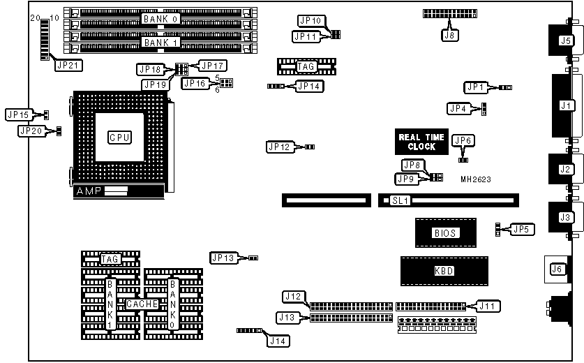
|
Processor |
Pentium |
|
Processor Speed |
75/90/100MHz |
|
Chip Set |
SIS |
|
Max. Onboard DRAM |
128MB |
|
Cache |
256/512/1024KB |
|
BIOS |
Phoenix |
|
Dimensions |
330mm x 218mm |
|
I/O Options |
Floppy drive interface, green PC connector, IDE interfaces (2), parallel port, PS/2 mouse port, serial ports (2), VGA feature connector, VGA port, riser slot |
|
NPU Options |
None |
|
CONNECTIONS | |||
|
Purpose |
Location |
Purpose |
Location |
|
Parallel port |
J1 |
3.3v connector |
J14 |
|
Serial port 2 |
J2 |
IDE interface LED |
JP15 |
|
Serial port 1 |
J3 |
Turbo LED |
JP21 pins 2 - 3 |
|
VGA port |
J5 |
Green PC connector |
JP21 pins 4 - 5 |
|
PS/2 mouse port |
J6 |
Turbo switch |
JP21 pins 6 - 7 |
|
VGA feature connector |
J8 |
Reset switch |
JP21 pins 9 - 10 |
|
Floppy drive interface |
J11 |
Power LED & keylock |
JP21 pins 11 - 15 |
|
IDE interface (secondary) |
J12 |
Speaker |
JP21 pins 17 - 20 |
|
IDE interface (primary) |
J13 |
Riser Card |
SL1 |
|
USER CONFIGURABLE SETTINGS | |||
|
Function |
Jumper |
Position | |
|
» |
Video memory type select fast page mode |
JP1 |
pins 1 & 2 closed |
|
Video memory type select extended data out mode |
JP1 |
pins 2 & 3 closed | |
|
» |
SMC 37C665 signal enabled |
JP4 |
pins 1 & 2 closed |
|
SMC 37C665 signal disabled |
JP4 |
pins 2 & 3 closed | |
|
» |
BIOS type select EPROM |
JP5 |
Open |
|
BIOS type select 5v flash |
JP5 |
pins 1 & 2 closed | |
|
BIOS type select 12v flash |
JP5 |
pins 2 & 3 closed | |
|
» |
CMOS memory normal operation |
JP6 |
Open |
|
CMOS memory clear |
JP6 |
Closed | |
|
» |
Parity check enabled |
JP12 |
pins 2 & 3 closed |
|
Parity check disabled |
JP12 |
pins 1 & 2 closed | |
|
» |
IDE interface enabled |
JP13 |
Open |
|
IDE interface disabled |
JP13 |
Closed | |
|
» |
DRAM type select single side in both banks |
JP14 |
pins 2 & 3 closed |
|
DRAM type select double side in bank 2 & single side in bank 1 |
JP14 |
pins 1 & 2, 3 & 4 closed | |
|
» |
Cache type select write back |
JP17 |
pins 1 & 2 closed |
|
Cache type select write through |
JP17 |
pins 2 & 3 closed | |
|
» |
CPU write to always |
JP18 |
pins 1 & 2 closed |
|
CPU write to invalidate |
JP18 |
pins 2 & 3 closed | |
|
» |
CPU next address disabled |
JP19 |
pins 1 & 2 closed |
|
CPU next address enabled |
JP19 |
pins 2 & 3 closed | |
|
» |
Factory configured - do not alter |
JP20 |
N/A |
|
DRAM CONFIGURATION | ||
|
Size |
Bank 0 |
Bank 1 |
|
2MB |
(2) 256K x 36 |
NONE |
|
4MB |
(2) 256K x 36 |
(2) 256K x 36 |
|
4MB |
(2) 512K x 36 |
NONE |
|
8MB |
(2) 512K x 36 |
(2) 512K x 36 |
|
8MB |
(2) 1M x 36 |
NONE |
|
16MB |
(2) 1M x 36 |
(2) 1M x 36 |
|
16MB |
(2) 2M x 36 |
NONE |
|
32MB |
(2) 2M x 36 |
(2) 2M x 36 |
|
36MB |
(2) 512K x 36 |
(2) 4M x 36 |
|
36MB |
(2) 512K x 36 |
(2) 4M x 36 |
|
48MB |
(2) 2M x 36 |
(2) 4M x 36 |
|
64MB |
(2) 4M x 36 |
(2) 4M x 36 |
|
64MB |
(2) 8M x 36 |
NONE |
|
128MB |
(2) 8M x 36 |
(2) 8M x 36 |
|
128MB |
(2) 16M x 36 |
NONE |
|
CACHE CONFIGURATION | |||
|
Size |
Bank 0 |
Bank 1 |
TAG |
|
256KB |
(4) 32K x 8 |
(4) 32K x 8 |
(2) 32K x 8 |
|
512KB |
(4) 64K x 8 |
(4) 64K x 8 |
(2) 32K x 8 |
|
1MB |
(4) 128K x 8 |
(4) 128K x 8 |
(2) 32K x 8 |
|
CACHE JUMPER CONFIGURATION | ||
|
Size |
JP10 |
JP11 |
|
256KB |
Open |
Open |
|
512KB |
Closed |
Open |
|
1MB |
Closed |
Closed |
|
CPU SPEED CONFIGURATION | |
|
Speed |
JP16 |
|
75MHz |
pins 1 & 2 closed |
|
90MHz |
pins 1 & 2, 5 & 6 closed |
|
100MHz |
pins 1 & 2, 3 & 4, 5 & 6 closed |
|
DACK/DRQ CONFIGURATION | ||
|
DACK/DRQ |
JP8 |
JP9 |
|
DACK1/DRQ1 |
pins 1 & 2 closed |
pins 1 & 2 closed |
|
DACK3/DRQ3 |
pins 2 & 3 closed |
pins 2 & 3 closed |