EURONE (HK) CO., LTD.
MS-5120
|
Processor |
CX 6X86/IBM 6X86/AM K5/AM K6/Pentium |
|
Processor Speed |
75/90/100/120/133/150/166/180/200MHz |
|
Chip Set |
Intel |
|
Video Chip Set |
None |
|
Maximum Onboard Memory |
256MB (EDO supported) |
|
Maximum Video Memory |
None |
|
Cache |
256/512KB |
|
BIOS |
Award |
|
Dimensions |
254mm x 218mm |
|
I/O Options |
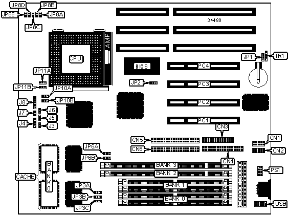
32-bit PCI slots (4), floppy drive interface, green PC connector, IDE interfaces (2), parallel port, PS/2 mouse interface, serial ports (2), IR connector, USB connector |
|
NPU Options |
None |
|
CONNECTIONS | |||
|
Purpose |
Location |
Purpose |
Location |
|
Serial port 1 |
CN1 |
Speaker |
J4 |
|
Serial port 2 |
CN2 |
Turbo LED |
J5 |
|
Parallel port |
CN3 |
Turbo switch |
J6 |
|
Floppy drive interface |
CN4 |
Reset switch |
J7 |
|
IDE interface 2 |
CN5 |
Power LED & keylock |
J8 |
|
IDE interface 1 |
CN6 |
32-bit PCI slots |
PC1 – PC4 |
|
IR connector |
IR1 |
PS/2 mouse interface |
PS1 |
|
IDE interface LED |
J3 |
USB connector |
USB |
|
USER CONFIGURABLE SETTINGS | |||
|
Function |
Label |
Position | |
|
» |
CMOS memory normal operation |
JP1 |
Open |
|
CMOS memory clear |
JP1 |
Closed | |
|
» |
Flash BIOS voltage select 12v |
JP2 |
Pins 1 & 2 closed |
|
Flash BIOS voltage select 5v |
JP2 |
Pins 2 & 3 closed | |
|
» |
Factory configured - do not alter (CPU voltage) |
JP8A |
Unidentified |
|
» |
Factory configured - do not alter (CPU voltage) |
JP8B |
Unidentified |
|
» |
Factory configured - do not alter (CPU voltage) |
JP8C |
Unidentified |
|
» |
Factory configured - do not alter (CPU voltage) |
JP8D |
Unidentified |
|
» |
Factory configured - do not alter (CPU voltage) |
JP8E |
Unidentified |
|
DRAM CONFIGURATION | ||
|
Size |
Bank 0 |
Bank 1 |
|
8MB |
(2) 1M x 36 |
None |
|
16MB |
(2) 2M x 36 |
None |
|
16MB |
(2) 1M x 36 |
(2) 1M x 36 |
|
24MB |
(2) 2M x 36 |
(2) 1M x 36 |
|
32MB |
(2) 4M x 36 |
None |
|
32MB |
(2) 2M x 36 |
(2) 2M x 36 |
|
40MB |
(2) 4M x 36 |
(2) 1M x 36 |
|
48MB |
(2) 4M x 36 |
(2) 2M x 36 |
|
64MB |
(2) 8M x 36 |
None |
|
64MB |
(2) 4M x 36 |
(2) 4M x 36 |
|
72MB |
(2) 8M x 36 |
(2) 1M x 36 |
|
80MB |
(2) 8M x 36 |
(2) 2M x 36 |
|
96MB |
(2) 8M x 36 |
(2) 4M x 36 |
|
128MB |
(2) 8M x 36 |
(2) 8M x 36 |
|
128MB |
(2) 16M x 36 |
None |
|
136MB |
(2) 16M x 36 |
(2) 1M x 36 |
|
144MB |
(2) 16M x 36 |
(2) 2M x 36 |
|
160MB |
(2) 16M x 36 |
(2) 4M x 36 |
|
192MB |
(2) 16M x 36 |
(2) 8M x 36 |
|
256MB |
(2) 16M x 36 |
(2) 16M x 36 |
|
DIMM CONFIGURATION | ||
|
Size |
Bank 0 |
Bank 1 |
|
8MB |
(1) 1M x 64 |
None |
|
16MB |
(1) 2M x 64 |
None |
|
16MB |
(1) 1M x 64 |
(1) 1M x 64 |
|
24MB |
(1) 2M x 64 |
(1) 1M x 64 |
|
32MB |
(1) 4M x 64 |
None |
|
32MB |
(1) 2M x 64 |
(1) 2M x 64 |
|
40MB |
(1) 4M x 64 |
(1) 1M x 64 |
|
48MB |
(1) 4M x 64 |
(1) 2M x 64 |
|
64MB |
(1) 8M x 64 |
None |
|
64MB |
(1) 4M x 64 |
(1) 4M x 64 |
|
72MB |
(1) 8M x 64 |
(1) 1M x 64 |
|
80MB |
(1) 8M x 64 |
(1) 2M x 64 |
|
96MB |
(1) 8M x 64 |
(1) 4M x 64 |
|
128MB |
(1) 8M x 64 |
(1) 8M x 64 |
|
Note: If DIMMs are used with SIMMs, SIMM bank 0 & DIMM bank 2 cannot be populated at the same time. | ||
|
DIMM VOLTAGE CONFIGURATION | ||
|
Voltage |
JP6A |
JP6B |
|
3.3v |
Pins 2 & 3 closed |
Pins 2 & 3 closed |
|
5v |
Pins 1 & 2 closed |
Pins 1 & 2 closed |
|
CACHE CONFIGURATION | |
|
Size |
Bank 0 |
|
256KB |
(2) 32K x 32 |
|
512KB |
(2) 64K x 32 |
|
CPU SPEED SELECTION (CYRIX) | |||||||
|
CPU speed |
Clock speed |
Multiplier |
JP3A |
JP3B |
JP3C |
JP11A |
JP11B |
|
150MHz |
60MHz |
2x |
2 & 3 |
2 & 3 |
1 & 2 |
2 & 3 |
1 & 2 |
|
200MHz |
66MHz |
2x |
2 & 3 |
1 & 2 |
2 & 3 |
2 & 3 |
1 & 2 |
|
Note: Pins designated should be in the closed position. | |||||||
|
CPU SPEED SELECTION (AMD) |
|
Note: The CPU speeds for the AMD processor is unidentified. |
|
CPU SPEED SELECTION (INTEL) | |||||||
|
CPU speed |
Clock speed |
Multiplier |
JP3A |
JP3B |
JP3C |
JP11A |
JP11B |
|
75MHz |
50MHz |
1.5x |
2 & 3 |
2 & 3 |
2 & 3 |
1 & 2 |
1 & 2 |
|
90MHz |
60MHz |
1.5x |
2 & 3 |
2 & 3 |
1 & 2 |
1 & 2 |
1 & 2 |
|
100MHz |
66MHz |
1.5x |
2 & 3 |
1 & 2 |
2 & 3 |
1 & 2 |
1 & 2 |
|
120MHz |
60MHz |
2x |
2 & 3 |
2 & 3 |
1 & 2 |
2 & 3 |
1 & 2 |
|
133MHz |
66MHz |
2x |
2 & 3 |
1 & 2 |
2 & 3 |
2 & 3 |
1 & 2 |
|
150MHz |
60MHz |
2.5x |
2 & 3 |
2 & 3 |
1 & 2 |
2 & 3 |
2 & 3 |
|
166MHz |
66MHz |
2.5x |
2 & 3 |
1 & 2 |
2 & 3 |
2 & 3 |
2 & 3 |
|
180MHz |
60MHz |
3x |
2 & 3 |
2 & 3 |
1 & 2 |
1 & 2 |
2 & 3 |
|
200MHz |
66MHz |
3x |
2 & 3 |
1 & 2 |
2 & 3 |
1 & 2 |
2 & 3 |
|
Note: Pins designated should be in the closed position. | |||||||
|
CPU TYPE SELECTION | ||
|
Type |
JP10A |
JP10B |
|
P54C |
Pins 1 & 2 closed |
Pins 1 & 2 closed |
|
P55C |
Pins 2 & 3 closed |
Pins 2 & 3 closed |