FLASH TECH, INC.
SL-66D
|
Device Type |
Mainboard |
|
Processor |
Pentium II/Celeron |
|
Processor Speed |
233/266/300/333MHz |
|
Chip Set |
Intel 440EX |
|
Maximum Onboard Memory |
256MB (EDO & SDRAM supported) |
|
Cache |
256/512KB (on the Pentium II CPU) |
|
BIOS |
Award |
|
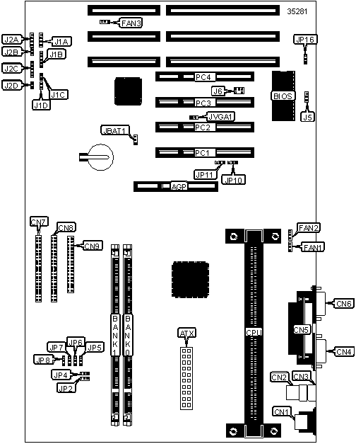
I/O Options |
32-bit PCI slots (4), floppy drive interface, IDE interfaces (2), parallel port, PS/2 mouse port, serial ports (2), AGP slot, USB ports (2), IR connector, green PC connector, ATX power connector |
|
Dimensions |
305mm x 170mm |
|
CONNECTIONS | |||
|
Purpose |
Location |
Purpose |
Location |
|
AGP slot |
AGP |
Chassis fan |
FAN3 |
|
ATX power connector |
ATX |
IDE interface LED |
J1A |
|
PS/2 mouse port |
CN1 |
IR connector |
J1B |
|
USB connector 2 |
CN2 |
Power switch |
J1C |
|
USB connector 1 |
CN3 |
SMI switch |
J1D |
|
Serial port 1 |
CN4 |
Speaker |
J2A |
|
Parallel port |
CN5 |
Reset switch |
J2B |
|
Serial port 2 |
CN6 |
Power LED & keylock |
J2C |
|
IDE interface 1 |
CN7 |
Turbo LED |
J2D |
|
IDE interface 2 |
CN8 |
Wake on LAN connector |
J5 |
|
Floppy drive interface |
CN9 |
SB Link |
J6 |
|
CPU fan |
FAN1 |
32-bit PCI slots |
PC1 - PC4 |
|
Power fan |
FAN2 | ||
|
USER CONFIGURABLE SETTINGS | |||
|
Function |
Label |
Position | |
|
» |
CMOS memory normal operation |
JBAT1 |
Pins 1 & 2 closed |
|
CMOS memory clear |
JBAT1 |
Pins 2 & 3 closed | |
|
» |
Normal VGA card enabled |
JVGA1 |
Closed |
|
Special VGA card enabled |
JVGA1 |
Open | |
|
» |
Power lost recovery normal |
JP16 |
Pins 2 & 3 closed |
|
Power lost recovery enabled |
JP16 |
Pins 1 & 2 closed | |
|
USB PORT SELECTION | |||
|
Function |
JP10 |
JP11 | |
| » |
Redirect USB1 to AGP port |
Pins 1 & 2 closed |
Pins 1 & 2 closed |
|
Redirect all USB ports to USB connector |
Pins 2 & 3 closed |
Pins 2 & 3 closed | |
|
DRAM CONFIGURATION | ||
|
Size |
Bank 0 |
Bank 1 |
|
8MB |
(1) 1MB x 64 |
None |
|
16MB |
(1) 1MB x 64 |
(1) 1MB x 64 |
|
16MB |
(1) 2MB x 64 |
None |
|
24MB |
(1) 2MB x 64 |
(1) 1MB x 64 |
|
32MB |
(1) 2MB x 64 |
(1) 2MB x 64 |
|
32MB |
(1) 4MB x 64 |
None |
|
40MB |
(1) 4MB x 64 |
(1) 1MB x 64 |
|
48MB |
(1) 4MB x 64 |
(1) 2MB x 64 |
|
64MB |
(1) 4MB x 64 |
(1) 4MB x 64 |
|
64MB |
(1) 8MB x 64 |
None |
|
72MB |
(1) 8MB x 64 |
(1) 1MB x 64 |
|
80MB |
(1) 8MB x 64 |
(1) 2MB x 64 |
|
96MB |
(1) 8MB x 64 |
(1) 4MB x 64 |
|
128MB |
(1) 8MB x 64 |
(1) 8MB x 64 |
|
136MB |
(1) 16MB x 64 |
None |
|
144MB |
(1) 16MB x 64 |
(1) 1MB x 64 |
|
160MB |
(1) 16MB x 64 |
(1) 2MB x 64 |
|
192MB |
(1) 16MB x 64 |
(1) 4MB x 64 |
|
224MB |
(1) 16MB x 64 |
(1) 8MB x 64 |
|
256MB |
(1) 16MB x 64 |
(1) 16MB x 64 |
|
Note: Board accepts both EDO and SDRAM. | ||
|
CACHE CONFIGURATION |
|
Note: 256/512KB cache is located on the Pentium II CPU. |
|
CPU SPEED SELECTION | ||||||||
|
CPU Speed |
Clock speed |
Multiplier |
JP2 |
JP4 |
JP5 |
JP6 |
JP7 |
JP8 |
|
233MHz |
66MHz |
3.5x |
1 & 2 |
1 & 2 |
2 & 3 |
Open |
Open |
2 & 3 |
|
266MHz |
66MHz |
4x |
1 & 2 |
1 & 2 |
Open |
2 & 3 |
2 & 3 |
2 & 3 |
|
300MHz |
66MHz |
4.5x |
1 & 2 |
1 & 2 |
Open |
2 & 3 |
Open |
2 & 3 |
|
333MHz |
66MHz |
5x |
1 & 2 |
1 & 2 |
Open |
Open |
2 & 3 |
2 & 3 |
|
Note: Numbers designate pins that should be closed. | ||||||||