ICL
CX386/cx386s/cx386s25/CX486/CX486(NEW)/CX486S25
|
Processor |
80386SX/80386DX/80486SX/80487SX/80486DX/80486DX2 (depends on CPU board installed) |
|
Processor Speed |
20/25/33/50(internal)/66(internal)MHz (depends on CPU board installed) |
|
Chip Set |
Symphony/Texas (depends on CPU board installed) |
|
Max. Onboard DRAM |
16/32MB (depends on CPU board installed) |
|
Cache |
None |
|
BIOS |
ICL |
|
Dimensions |
220mm x 180mm |
|
I/O Options |
PS/2 mouse port (on CPU board), serial ports (2), parallel port, IDE interface, floppy drive interface |
|
NPU Options |
4167 |
|
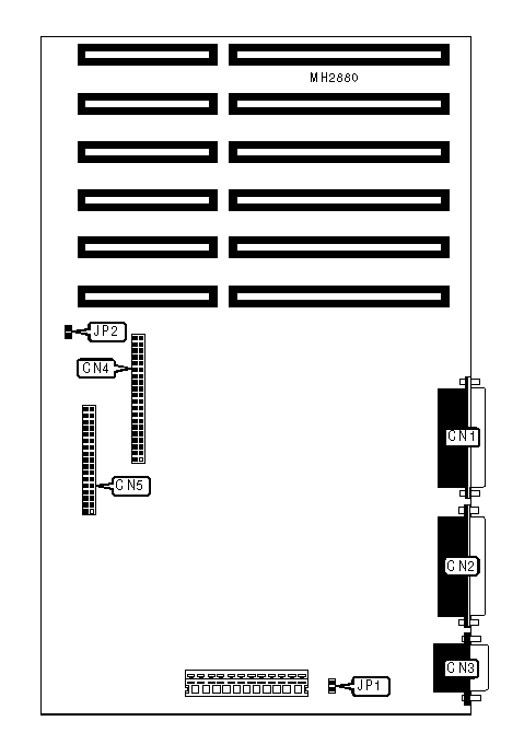
CONNECTIONS | |||
|
Purpose |
Location |
Purpose |
Location |
|
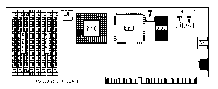
Parallel port |
CN1 |
Floppy drive interface |
CN5 |
|
Serial port 2 |
CN2 |
Chassis fan power |
JP1 |
|
Serial port 1 |
CN3 |
IDE interface LED |
JP2 |
|
IDE interface |
CN4 | ||
|
CONNECTIONS | |
|
Purpose |
Location |
|
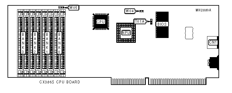
PS/2 mouse port |
CN1 |
|
USER CONFIGURABLE SETTINGS | |||
|
Function |
Jumper |
Position | |
|
» |
Factory configured - do not alter |
T01A |
N/A |
|
» |
Factory configured - do not alter |
W04 |
N/A |
|
» |
CMOS memory normal operation |
W05 |
pins 1 & 2 closed |
|
CMOS memory clear |
W05 |
pins 2 & 3 closed | |
|
DRAM CONFIGURATION | ||||
|
Size |
Bank 0 |
Bank 1 |
Bank 2 |
Bank 3 |
|
1MB |
(2) 256K x 9 |
(2) 256K x 9 |
NONE |
NONE |
|
1.5MB |
(2) 256K x 9 |
(2) 256K x 9 |
(2) 256K x 9 |
NONE |
|
2MB |
(2) 256K x 9 |
(2) 256K x 9 |
(2) 256K x 9 |
(2) 256K x 9 |
|
2MB |
(2) 1M x 9 |
NONE |
NONE |
NONE |
|
3MB |
(2) 256K x 9 |
(2) 256K x 9 |
(2) 1M x 9 |
NONE |
|
4MB |
(2) 1M x 9 |
(2) 1M x 9 |
NONE |
NONE |
|
5MB |
(2) 256K x 9 |
(2) 256K x 9 |
(2) 1M x 9 |
(2) 1M x 9 |
|
6MB |
(2) 1M x 9 |
(2) 1M x 9 |
(2) 1M x 9 |
NONE |
|
DRAM CONFIGURATION (CON’T) | ||||
|
Size |
Bank 0 |
Bank 1 |
Bank 2 |
Bank 3 |
|
8MB |
(2) 1M x 9 |
(2) 1M x 9 |
(2) 1M x 9 |
(2) 1M x 9 |
|
8MB |
(2) 4M x 9 |
NONE |
NONE |
NONE |
|
10MB |
(2) 1M x 9 |
NONE |
(2) 4M x 9 |
NONE |
|
12MB |
(2) 1M x 9 |
(2) 1M x 9 |
(2) 4M x 9 |
NONE |
|
16MB |
(2) 4M x 9 |
(2) 4M x 9 |
NONE |
NONE |
|
CONNECTIONS | |||
|
Purpose |
Location |
Purpose |
Location |
|
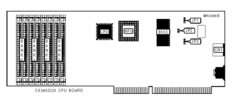
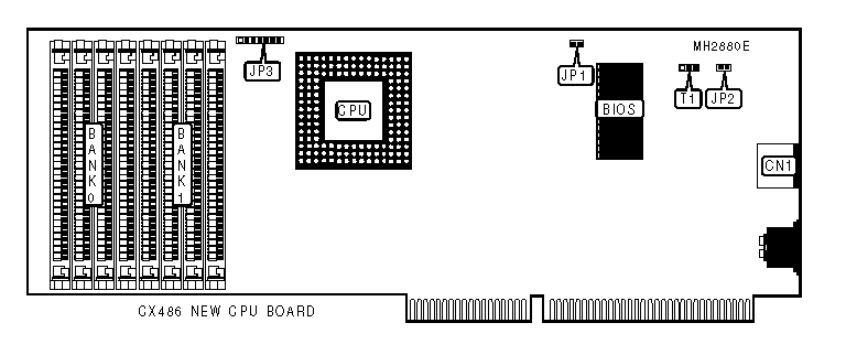
PS/2 mouse port |
CN1 |
Reset switch |
JP2 |
|
USER CONFIGURABLE SETTINGS | |||
|
Function |
Jumper |
Position | |
|
» |
Factory configured - do not alter |
JP1 |
N/A |
|
» |
CMOS memory normal operation |
JP3 |
pins 2 & 3 closed |
|
CMOS memory clear |
JP3 |
pins 1 & 2 closed | |
|
DRAM CONFIGURATION | ||||
|
Size |
Bank 0 |
Bank 1 |
Bank 2 |
Bank 3 |
|
1MB |
(2) 256K x 9 |
(2) 256K x 9 |
NONE |
NONE |
|
1.5MB |
(2) 256K x 9 |
(2) 256K x 9 |
(2) 256K x 9 |
NONE |
|
2MB |
(2) 256K x 9 |
(2) 256K x 9 |
(2) 256K x 9 |
(2) 256K x 9 |
|
2MB |
(2) 1M x 9 |
NONE |
NONE |
NONE |
|
3MB |
(2) 256K x 9 |
(2) 256K x 9 |
(2) 1M x 9 |
NONE |
|
4MB |
(2) 1M x 9 |
(2) 1M x 9 |
NONE |
NONE |
|
5MB |
(2) 256K x 9 |
(2) 256K x 9 |
(2) 1M x 9 |
(2) 1M x 9 |
|
6MB |
(2) 1M x 9 |
(2) 1M x 9 |
(2) 1M x 9 |
NONE |
|
DRAM CONFIGURATION (CON’T) | ||||
|
Size |
Bank 0 |
Bank 1 |
Bank 2 |
Bank 3 |
|
8MB |
(2) 1M x 9 |
(2) 1M x 9 |
(2) 1M x 9 |
(2) 1M x 9 |
|
8MB |
(2) 4M x 9 |
NONE |
NONE |
NONE |
|
10MB |
(2) 1M x 9 |
NONE |
(2) 4M x 9 |
NONE |
|
12MB |
(2) 1M x 9 |
(2) 1M x 9 |
(2) 4M x 9 |
NONE |
|
16MB |
(2) 4M x 9 |
(2) 4M x 9 |
NONE |
NONE |
|
CONNECTIONS | |
|
Purpose |
Location |
|
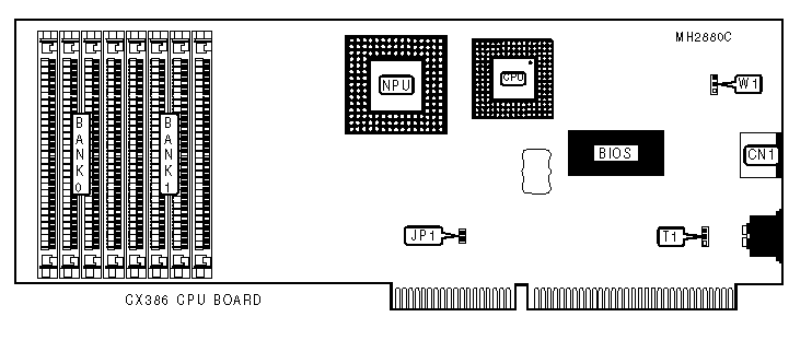
PS/2 mouse port |
CN1 |
|
USER CONFIGURABLE SETTINGS | |||
|
Function |
Jumper |
Position | |
|
» |
Factory configured - do not alter |
JP1 |
N/A |
|
» |
Factory configured - do not alter |
T1 |
N/A |
|
» |
CMOS memory normal operation |
W1 |
pins 2 & 3 closed |
|
CMOS memory clear |
W1 |
pins 1 & 2 closed | |
|
DRAM CONFIGURATION | ||
|
Size |
Bank 0 |
Bank 1 |
|
4MB |
(4) 1M x 9 |
NONE |
|
8MB |
(4) 1M x 9 |
(4) 1M x 9 |
|
16MB |
(4) 4M x 9 |
NONE |
|
20MB |
(4) 4M x 9 |
(4) 1M x 9 |
|
32MB |
(4) 4M x 9 |
(4) 4M x 9 |
|
CONNECTIONS | |
|
Purpose |
Location |
|
PS/2 mouse port |
CN1 |
|
USER CONFIGURABLE SETTINGS | |||
|
Function |
Jumper |
Position | |
|
» |
CMOS memory normal operation |
JP1 |
Open |
|
CMOS memory clear |
JP1 |
Closed | |
|
» |
Factory configured - do not alter |
JP2 |
N/A |
|
» |
Factory configured - do not alter |
T1 |
N/A |
|
DRAM CONFIGURATION | ||
|
Size |
Bank 0 |
Bank 1 |
|
4MB |
(4) 1M x 9 |
NONE |
|
8MB |
(4) 1M x 9 |
(4) 1M x 9 |
|
16MB |
(4) 4M x 9 |
NONE |
|
20MB |
(4) 4M x 9 |
(4) 1M x 9 |
|
32MB |
(4) 4M x 9 |
(4) 4M x 9 |
|
NPU CONFIGURATION | |
|
Type |
JP3 |
|
ODP486SX-25 |
pins 2 & 3, 6 & 7 closed |
|
80487SX |
pins 2 & 3, 6 & 7 closed |
|
CONNECTIONS | |
|
Purpose |
Location |
|
PS/2 mouse port |
CN1 |
|
USER CONFIGURABLE SETTINGS | |||
|
Function |
Jumper |
Position | |
|
» |
CMOS memory normal operation |
JP1 |
Open |
|
CMOS memory clear |
JP1 |
Closed | |
|
» |
Factory configured - do not alter |
JP2 |
N/A |
|
» |
Factory configured - do not alter |
T1 |
N/A |
|
DRAM CONFIGURATION | ||
|
Size |
Bank 0 |
Bank 1 |
|
4MB |
(4) 1M x 9 |
NONE |
|
8MB |
(4) 1M x 9 |
(4) 1M x 9 |
|
16MB |
(4) 4M x 9 |
NONE |
|
20MB |
(4) 4M x 9 |
(4) 1M x 9 |
|
32MB |
(4) 4M x 9 |
(4) 4M x 9 |
|
CPU TYPE CONFIGURATION | |
|
Type |
JP3 |
|
ODP486SX |
pins 2 & 3, 6 & 7 closed |
|
ODPR486 |
pins 1 & 2, 5 & 6 closed |
|
80486DX |
pins 1 & 2, 5 & 6 closed |
|
80486DX2 |
pins 1 & 2, 5 & 6 closed |

|
CONNECTIONS | |
|
Purpose |
Location |
|
PS/2 mouse port |
CN1 |
|
USER CONFIGURABLE SETTINGS | |||
|
Function |
Jumper |
Position | |
|
» |
Factory configured - do not alter |
J1 |
N/A |
|
» |
Factory configured - do not alter |
J2 |
N/A |
|
» |
Factory configured - do not alter |
J3 |
N/A |
|
» |
Factory configured - do not alter |
J4 |
N/A |
|
» |
Factory configured - do not alter |
J5 |
N/A |
|
» |
CMOS memory normal operation |
J13 |
Open |
|
CMOS memory clear |
J13 |
Closed | |
|
DRAM CONFIGURATION | ||
|
Size |
Bank 0 |
Bank 1 |
|
4MB |
(4) 1M x 9 |
NONE |
|
8MB |
(4) 1M x 9 |
(4) 1M x 9 |
|
16MB |
(4) 4M x 9 |
NONE |
|
20MB |
(4) 4M x 9 |
(4) 1M x 9 |
|
32MB |
(4) 4M x 9 |
(4) 4M x 9 |