ICL
CS486S
|
Processor |
80487SX/80486DX |
|
Processor Speed |
20/33MHz |
|
Chip Set |
Unidentified |
|
Max. Onboard DRAM |
26MB |
|
Cache |
None |
|
BIOS |
ICL |
|
Dimensions |
330mm x 218mm |
|
I/O Options |
PS/2 mouse port, parallel port, serial ports (2), VGA port, floppy drive interface, IDE interface |
|
NPU Options |
None |
|
CONNECTIONS | |||
|
Purpose |
Location |
Purpose |
Location |
|
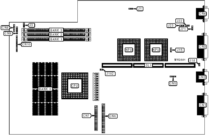
Parallel port |
CN1 |
Floppy drive interface |
CN7 |
|
Serial port 1 |
CN2 |
PS/2 mouse connector |
CN8 |
|
Serial port 2 |
CN3 |
Keyboard connector |
CN9 |
|
VGA port |
CN4 |
Front panel connector |
CN10 |
|
External battery |
CN5 |
Riser slot |
SL1 |
|
IDE interface |
CN6 | ||
|
USER CONFIGURABLE SETTINGS | |||
|
Function |
Jumper/Switch |
Position | |
|
» |
On board VGA enabled |
J1 |
pins 1 & 2 closed |
|
On board VGA disabled |
J1 |
pins 2 & 3 closed | |
|
» |
Factory configured - do not alter |
J2 |
pins 1 & 2 closed |
|
» |
Factory configured - do not alter |
J3 |
pins 1 & 2 closed |
|
» |
Factory configured - do not alter |
J4 |
Closed |
|
» |
Factory configured - do not alter |
J5 |
pins 1 & 2 closed |
|
» |
Factory configured - do not alter |
J6 |
pins 1 & 2 closed |
|
» |
Factory configured - do not alter |
J7 |
pins 2 & 3 closed |
|
» |
BIOS type select 27512 |
J15 |
pins 1 & 2 closed |
|
BIOS type select 27256 |
J15 |
pins 2 & 3 closed | |
|
» |
CMOS memory normal operation |
J18 |
Open |
|
CMOS memory clear |
J18 |
Closed | |
|
» |
VGA uses 0 wait states |
J22 |
pins 2 & 3 closed |
|
VGA uses IRQ9 |
J22 |
pins 1 & 2 closed | |
|
» |
ATREF# enabled |
J23 |
pins 1 & 2 closed |
|
ATREF# disabled |
J23 |
pins 2 & 3 closed | |
|
» |
BIOS bit select 8-bit BIOS |
J71 |
pins 2 & 3 closed |
|
BIOS bit select 16-bit BIOS |
J71 |
pins 1 & 2 closed | |
|
» |
Floppy drive interface enabled |
SW1/1 |
On |
|
Floppy drive interface disabled |
SW1/1 |
Off | |
|
» |
IDE interface enabled |
SW1/2 |
On |
|
IDE interface disabled |
SW1/2 |
Off | |
|
» |
Serial port 1 enabled |
SW1/3 |
On |
|
Serial port 1 disabled |
SW1/3 |
Off | |
|
» |
Serial port 2 enabled |
SW1/4 |
On |
|
Serial port 2 disabled |
SW1/4 |
Off | |
|
» |
Parallel port enabled |
SW1/5 |
On |
|
Parallel port disabled |
SW1/5 |
Off | |
|
» |
Memory 0F0000H-0FFFFFFH available for expansion |
SW1/6 |
Off |
|
Memory 0F0000H-0FFFFFFH reserved for system board |
SW1/6 |
On | |
|
» |
Reset disabled |
SW1/7 |
Off |
|
Reset enabled |
SW1/7 |
On | |
|
» |
Password disabled |
SW1/8 |
On |
|
Password enabled |
SW1/8 |
Off | |
|
Note: The location of jumpers J2, J4, J5, J6, &J7 and SW1 are unidentified. | |||
|
DRAM CONFIGURATION | ||||
|
Size |
Bank 0 |
Bank 1 |
Bank 2 |
Bank 3 |
|
2MB |
2MB |
NONE |
NONE |
NONE |
|
4MB |
2MB |
(1) 512K x 36 |
NONE |
NONE |
|
6MB |
2MB |
(1) 512K x 36 |
(1) 512K x 36 |
NONE |
|
6MB |
2MB |
(1) 1M x 36 |
NONE |
NONE |
|
8MB |
2MB |
(1) 512K x 36 |
(1) 512K x 36 |
(1) 512K x 36 |
|
8MB |
2MB |
(1) 512K x 36 |
(1) 1M x 36 |
NONE |
|
10MB |
2MB |
(1) 512K x 36 |
(1) 512K x 36 |
(1) 1M x 36 |
|
10MB |
2MB |
(1) 2M x 36 |
NONE |
NONE |
|
12MB |
2MB |
(1) 512K x 36 |
(1) 2M x 36 |
NONE |
|
14MB |
2MB |
(1) 512K x 36 |
(1) 512K x 36 |
(1) 2M x 36 |
|
14MB |
2MB |
(1) 1M x 36 |
(1) 2M x 36 |
NONE |
|
16MB |
2MB |
(1) 512K x 36 |
(1) 1M x 36 |
(1) 2M x 36 |
|
18MB |
2MB |
(1) 2M x 36 |
(1) 2M x 36 |
NONE |
|
20MB |
2MB |
(1) 512K x 36 |
(1) 2M x 36 |
(1) 2M x 36 |
|
22MB |
2MB |
(1) 1M x 36 |
(1) 2M x 36 |
(1) 2M x 36 |
|
26MB |
2MB |
(1) 2M x 36 |
(1) 2M x 36 |
(1) 2M x 36 |
|
Note: Bank 0 is factory installed and is not configurable. | ||||
|
CPU SPEED CONFIGURATION | |
|
Speed |
JP102 |
|
20MHz |
Closed |
|
33MHz |
Open |