LASER COMPUTER, INC.
LASER 386M
|
Processor |
80386SX |
|
Processor Speed |
25/33MHz |
|
Chip Set |
Unidentified |
|
Max. Onboard DRAM |
12MB |
|
Cache |
Unidentified |
|
BIOS |
Unidentified |
|
Dimensions |
330mm x 218mm |
|
I/O Options |
None |
|
NPU Options |
80387SX |
|
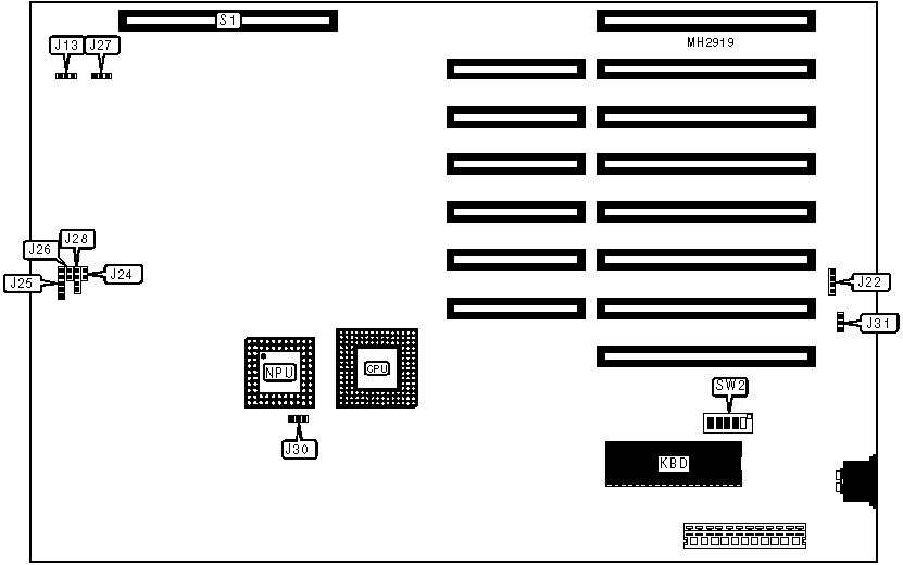
CONNECTIONS | |||
|
Purpose |
Location |
Purpose |
Location |
|
External battery |
J22 |
Turbo switch |
J26 |
|
Reset switch |
J24 |
Speaker |
J28 |
|
Power LED & keylock |
J25 |
External memory card |
S1 |
|
USER CONFIGURABLE SETTINGS | |||
|
Function |
Jumper/Switch |
Position | |
|
» |
EPROM chip type select 27128 or 2764 |
J13 |
pins 2 & 3 closed |
|
EPROM chip type select 27256 |
J13 |
pins 1 & 2 closed | |
|
» |
SYSCLK enabled |
J30 |
pins 2 & 3 closed |
|
SYSCLK disabled |
J30 |
pins 1 & 2 closed | |
|
» |
Battery type select internal |
J31 |
pins 1 & 2 closed |
|
Battery type select external |
J31 |
pins 2 & 3 closed | |
|
» |
EGA BIOS access select on board |
SW2/1 |
On |
|
EGA BIOS access select adapter card |
SW2/1 |
Off | |
|
» |
Memory type select 513KB to 640KB expansion bus enabled |
SW2/2 |
On |
|
Memory type select expansion bus disabled |
SW2/2 |
Off | |
|
» |
NPU disabled |
SW2/3 |
On |
|
NPU enabled |
SW2/3 |
Off | |
|
» |
Clock frequency speed select 25/33Mhz |
SW2/4 |
Off |
|
Clock frequency speed select 8Mhz |
SW2/4 |
On | |
|
» |
Monitor type select monochrome |
SW2/5 |
Off |
|
Monitor type select color |
SW2/5 |
On | |
|
CACHE CONFIGURATION | |
|
Setting |
J27 |
|
Enabled |
pins 2 & 3 closed |
|
Disabled |
pins 1 & 2 closed |
|
Note: The size and location of the cache is unidentified. | |
|
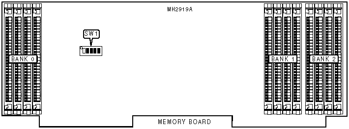
DRAM CONFIGURATION | |||
|
Size |
Bank 0 |
Bank 1 |
Bank 2 |
|
1MB |
(4) 256K x 9 |
NONE |
NONE |
|
2MB |
(4) 256K x 9 |
(4) 256K x 9 |
NONE |
|
3MB |
(4) 256K x 9 |
(4) 256K x 9 |
(4) 256K x 9 |
|
4MB |
(4) 1M x 9 |
NONE |
NONE |
|
5MB |
(4) 256K x 9 |
(4) 1M x 9 |
NONE |
|
6MB |
(4) 256K x 9 |
(4) 256K x 9 |
(4) 1M x 9 |
|
8MB |
(4) 1M x 9 |
(4) 1M x 9 |
NONE |
|
9MB |
(4) 256K x 9 |
(4) 1M x 9 |
(4) 1M x 9 |
|
12MB |
(4) 1M x 9 |
(4) 1M x 9 |
(4) 1M x 9 |
|
DRAM SWITCH CONFIGURATION | ||||
|
Size |
SW1/1 |
SW1/2 |
SW1/3 |
SW1/4 |
|
1MB |
On |
Off |
On |
On |
|
2MB |
Off |
On |
On |
On |
|
3MB |
Off |
Off |
On |
On |
|
4MB |
On |
Off |
On |
Off |
|
5MB |
Off |
On |
Off |
On |
|
6MB |
Off |
Off |
Off |
Off |
|
8MB |
Off |
On |
On |
Off |
|
9MB |
Off |
Off |
Off |
On |
|
12MB |
Off |
Off |
On |
Off |
|
MEMORY RELOCATION CONFIGURATION | |
|
Setting |
SW2/5 |
|
Enabled |
On |
|
Disabled |
Off |
|
TECHNICAL NOTE |
|
Note: The location of pin 1 is unidentified. |