ICL
TEAMSERVER FI
|
Processor |
Pentium |
|
Processor Speed |
75/100MHz |
|
Chip Set |
Unidentified |
|
Video Chip Set |
None |
|
Maximum Onboard Memory |
256MB |
|
Maximum Video Memory |
None |
|
Cache |
256/512KB |
|
BIOS |
Unidentified |
|
Dimensions |
355mm x 304mm |
|
I/O Options |
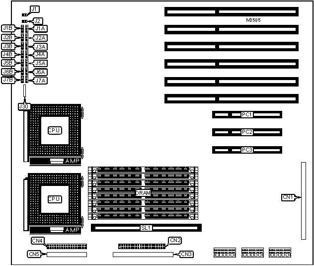
32-bit PCI slots (3), floppy drive interface, IDE interface, parallel port, VGA port, PS/2 mouse port, backplane connector, riser board, cache slot |
|
NPU Options |
None |
|
CONNECTIONS | |||
|
Purpose |
Location |
Purpose |
Location |
|
Riser board |
CN1 |
Front panel connector |
CN5 |
|
IDE interface (not used) |
CN2 |
Speaker/reset switch |
J30 |
|
Backplane connector |
CN3 |
32-bit PCI slots |
PC1 - PC3 |
|
Floppy drive interface |
CN4 |
Cache slot |
SL1 |
|
Note: Parallel port, VGA port and mouse port are located on the riser board. | |||
|
USER CONFIGURABLE SETTINGS | |||
|
Function |
Label |
Position | |
|
» |
Factory configured - do not alter |
J1 |
Unidentified |
|
» |
Factory configured - do not alter |
J2 |
Unidentified |
|
» |
Factory configured - do not alter |
J1A |
Pins 1 & 2 closed |
|
» |
CMOS memory normal operation |
J1B |
Pins 1 & 2 closed |
|
CMOS memory clear |
J1B |
Pins 2 & 3 closed | |
|
» |
Password normal operation |
J2B |
Pins 1 & 2 closed |
|
Password clear |
J2B |
Pins 2 & 3 closed | |
|
» |
CPU socket 1 set as primary socket |
J3B |
Pins 1 & 2 closed |
|
CPU socket 2 set as primary socket |
J3B |
Pins 2 & 3 closed | |
|
» |
Monitor type select color |
J4A |
Pins 1 & 2 closed |
|
Monitor type select monochrome |
J4A |
Pins 2 & 3 closed | |
|
» |
Factory configured - do not alter (disable & ground) |
J4B |
Pins 1 & 2 closed |
|
» |
Factory configured - do not alter (enable & kickstart) |
J4B |
Pins 2 & 3 closed |
|
» |
Flash BIOS write protect enabled |
J5A |
Pins 1 & 2 closed |
|
Flash BIOS write protect disabled |
J5A |
Pins 2 & 3 closed | |
|
» |
Flash BIOS access to system configuration utility enabled |
J6A |
Pins 1 & 2 closed |
|
Flash BIOS access to system configuration utility disabled |
J6A |
Pins 2 & 3 closed | |
|
» |
Flash BIOS normal operation |
J7A |
Pins 1 & 2 closed |
|
Flash BIOS recovery mode |
J7A |
Pins 2 & 3 closed | |
|
» |
Factory configured - do not alter |
J7B |
Pins 1 & 2 closed |
|
DRAM CONFIGURATION | ||||
|
Size |
Bank 0 |
Bank 1 |
Bank 2 |
Bank 3 |
|
16MB |
(2) 2M x 36 |
None |
None |
None |
|
32MB |
(2) 2M x 36 |
(2) 2M x 36 |
None |
None |
|
32MB |
(2) 4M x 36 |
None |
None |
None |
|
48MB |
(2) 2M x 36 |
(2) 2M x 36 |
(2) 2M x 36 |
None |
|
48MB |
(2) 4M x 36 |
(2) 2M x 36 |
None |
None |
|
64MB |
(2) 2M x 36 |
(2) 2M x 36 |
(2) 2M x 36 |
(2) 2M x 36 |
|
64MB |
(2) 4M x 36 |
(2) 4M x 36 |
None |
None |
|
64MB |
(2) 8M x 36 |
None |
None |
None |
|
64MB |
(2) 4M x 36 |
(2) 2M x 36 |
(2) 2M x 36 |
None |
|
80MB |
(2) 4M x 36 |
(2) 2M x 36 |
(2) 2M x 36 |
(2) 2M x 36 |
|
80MB |
(2) 8M x 36 |
(2) 2M x 36 |
None |
None |
|
DRAM CONFIGURATION (CON’T) | ||||
|
Size |
Bank 0 |
Bank 1 |
Bank 2 |
Bank 3 |
|
96MB |
(2) 4M x 36 |
(2) 4M x 36 |
(2) 4M x 36 |
None |
|
96MB |
(2) 8M x 36 |
(2) 2M x 36 |
(2) 2M x 36 |
None |
|
96MB |
(2) 8M x 36 |
(2) 4M x 36 |
None |
None |
|
112MB |
(2) 8M x 36 |
(2) 2M x 36 |
(2) 2M x 36 |
(2) 2M x 36 |
|
128MB |
(2) 4M x 36 |
(2) 4M x 36 |
(2) 4M x 36 |
(2) 4M x 36 |
|
128MB |
(2) 8M x 36 |
(2) 8M x 36 |
None |
None |
|
128MB |
(2) 8M x 36 |
(2) 4M x 36 |
(2) 4M x 36 |
None |
|
160MB |
(2) 8M x 36 |
(2) 4M x 36 |
(2) 4M x 36 |
(2) 4M x 36 |
|
192MB |
(2) 8M x 36 |
(2) 8M x 36 |
(2) 8M x 36 |
None |
|
256MB |
(2) 8M x 36 |
(2) 8M x 36 |
(2) 8M x 36 |
(2) 8M x 36 |
|
Note: The location of banks 0, 1, 2 & 3 are unidentified. | ||||
|
CACHE CONFIGURATION | |
|
Size |
SL1 |
|
256KB |
256KB module installed |
|
512KB |
512KB module installed |
|
CPU SPEED SELECTION | ||
|
Speed |
J5B |
J6B |
|
50MHz |
Pins 1 & 2 closed |
Pins 2 & 3 closed |
|
60MHz |
Pins 1 & 2 closed |
Pins 1 & 2 closed |
|
66MHz |
Pins 2 & 3 closed |
Pins 2 & 3 closed |
|
CPU TYPE SELECTION | |
|
Type |
J2A |
|
P54C |
Pins 1 & 2 closed |
|
P54CS |
Pins 2 & 3 closed |
|
CPU VOLTAGE SELECTION | |
|
Voltage |
J3A |
|
Standard or VR |
Pins 1 & 2 closed |
|
VRE |
Pins 2 & 3 closed |