INTEL CORPORATION
RU430HX
|
Processor |
Pentium |
|
Processor Speed |
75/90/100/120/133/150/166/180/200MHz |
|
Chip Set |
Intel |
|
Video Chip Set |
S3 |
|
Maximum Onboard Memory |
128MB (EDO supported) |
|
Maximum Video Memory |
2MB |
|
Cache |
256/512KB |
|
BIOS |
AMI |
|
Dimensions |
229mm x 219mm |
|
I/O Options |
CD-ROM connector, floppy drive interface, green PC connector, IDE interfaces (2), parallel port, PS/2 mouse port, serial ports (2), VESA feature connector, VGA port, riser slot, IR connectors (2), serial port/USB connector, microphone in connector, line out connector, MIDI/audio input connector, wave table connector, telephony connector |
|
NPU Options |
None |
|
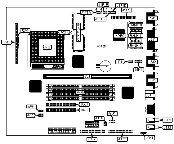
CONNECTIONS | |||
|
Purpose |
Location |
Purpose |
Location |
|
VESA feature connector |
J1G1 |
Serial port/USB connector |
J5J2 |
|
VGA port |
J1J1 |
Serial port 1 |
J6J1 |
|
IDE interface LED |
J2A1 pins 1 & 2 |
Soft off connector |
J8B1 |
|
Reset switch |
J2A1 pins 3 & 4 |
IDE interface 2 |
J8C1 |
|
IR connector |
J2A1 pins 6 - 9 |
IDE interface 1 |
J8C2 |
|
Chassis fan power |
J2A2 pins 1 & 2 |
PS/2 mouse port |
J8J1 |
|
Reset switch |
J2A2 pins 4 & 5 |
Microphone in connector |
J8J2 |
|
Power LED & keylock |
J2A2 pins 7 - 10 |
Line out connector |
J8J3 |
|
IDE interface LED |
J2A2 pins 11 - 14 |
Floppy drive interface |
J9E2 |
|
Soft on power connector |
J2A2 pins 15 & 16 |
Telephony connector |
J9F1 |
|
Green PC connector |
J2A2 pins 17 & 18 |
Wave table connector |
J9G1 |
|
IR connector |
J2A2 pins 20 - 25 |
MIDI/audio input connector |
J9G2 |
|
Speaker |
J2A2 pins 26 - 29 |
CD-ROM connector |
J9H1 |
|
Parallel port |
J3J1 |
Riser slot |
SL1 |
|
Serial port 2 |
J5H1 | ||
|
USER CONFIGURABLE SETTINGS | |||
|
Function |
Label |
Position | |
|
» |
Password normal operation |
J1F1A |
Pins 1 & 2 closed |
|
Password clear |
J1F1A |
Pins 2 & 3 closed | |
|
» |
CMOS memory normal operation |
J1F1A |
Pins 4 & 5 closed |
|
CMOS memory clear |
J1F1A |
Pins 5 & 6 closed | |
|
» |
Setup access enabled |
J1F1B |
Pins 1 & 2 closed |
|
Setup access disabled |
J1F1B |
Pins 2 & 3 closed | |
|
» |
Factory configured - do not alter |
JP1 |
Unidentified |
|
» |
Factory configured - do not alter |
JP2 |
Unidentified |
|
DRAM CONFIGURATION | ||
|
Size |
Bank 0 |
Bank 1 |
|
8MB |
(2) 1M x 36 |
None |
|
16MB |
(2) 2M x 36 |
None |
|
16MB |
(2) 1M x 36 |
(2) 1M x 36 |
|
24MB |
(2) 2M x 36 |
(2) 1M x 36 |
|
32MB |
(2) 4M x 36 |
None |
|
32MB |
(2) 2M x 36 |
(2) 2M x 36 |
|
40MB |
(2) 4M x 36 |
(2) 1M x 36 |
|
48MB |
(2) 4M x 36 |
(2) 2M x 36 |
|
DRAM CONFIGURATION (CON’T) | ||
|
Size |
Bank 0 |
Bank 1 |
|
64MB |
(2) 8M x 36 |
None |
|
64MB |
(2) 4M x 36 |
(2) 4M x 36 |
|
72MB |
(2) 8M x 36 |
(2) 1M x 36 |
|
80MB |
(2) 8M x 36 |
(2) 2M x 36 |
|
96MB |
(2) 8M x 36 |
(2) 4M x 36 |
|
128MB |
(2) 8M x 36 |
(2) 8M x 36 |
|
Note: Board accepts EDO memory. Board also accepts x 32 SIMMs. The location of banks 0 & 1 are unidentified. | ||
|
CACHE CONFIGURATION | |
|
Size |
Bank 0 |
|
256KB |
(2) 32K x 32 |
|
512KB |
(2) 64K x 32 |
|
Note: Board will come factory installed with one of the two above cache sizes. | |
|
VIDEO MEMORY CONFIGURATION | ||
|
Size |
Bank 0 |
Bank 1 |
|
1MB |
1MB |
None |
|
2MB |
1MB |
(2) 256K x 16 |
|
Note: Bank 0 is factory installed and is not configurable. | ||
|
CPU SPEED SELECTION | ||||
|
CPU speed |
Clock speed |
Multiplier |
J1F1C |
J1F1D |
|
75MHz |
50MHz |
1.5x |
2 & 3, 5 & 6 |
1 & 2, 4 & 5 |
|
90MHz |
60MHz |
1.5x |
2 & 3, 5 & 6 |
1 & 2, 4 & 5 |
|
100MHz |
66MHz |
1.5x |
1 & 2, 5 & 6 |
1 & 2, 4 & 5 |
|
120MHz |
60MHz |
2x |
2 & 3, 4 & 5 |
2 & 3, 4 & 5 |
|
133MHz |
66MHz |
2x |
1 & 2, 5 & 6 |
2 & 3, 4 & 5 |
|
150MHz |
60MHz |
2.5x |
2 & 3, 4 & 5 |
2 & 3, 5 & 6 |
|
166MHz |
66MHz |
2.5x |
1 & 2, 5 & 6 |
2 & 3, 5 & 6 |
|
180MHz |
60MHz |
3x |
2 & 3, 4 & 5 |
1 & 2, 5 & 6 |
|
200MHz |
66MHz |
3x |
1 & 2, 5 & 6 |
1 & 2, 5 & 6 |
|
Note: Pins designated should be in the closed position. | ||||
|
CPU TYPE SELECTION | |
|
Type |
J1F1B |
|
Standard or VR |
Pins 4 & 5 closed |
|
VRE |
Pins 5 & 6 closed |