IBM CORPORATION
APTIVA 2144, 2168 TYPE H-2, I-2
|
Processor |
CX M1/Pentium |
|
Processor Speed |
75/90/100/120/133/150/166MHz |
|
Chip Set |
Unidentified |
|
Video Chip Set |
Unidentified |
|
Maximum Onboard Memory |
128MB (EDO supported) |
|
Maximum Video Memory |
2MB |
|
Cache |
256/512KB |
|
BIOS |
Unidentified |
|
Dimensions |
330mm x 218mm |
|
I/O Options |
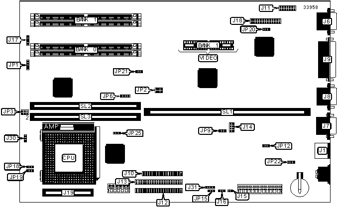
Floppy drive interface, IDE interfaces (2), parallel port, PS/2 mouse port, ports (2), VESA feature connector, VGA port, VGA interface, riser slot, cache slots (2), VRM connector, modem wake up connector, power supply connectors (2) |
|
NPU Options |
None |
|
CONNECTIONS | |||
|
Purpose |
Location |
Purpose |
Location |
|
PS/2 mouse port |
J1 |
32-bit PCI slots |
J16 |
|
VGA port |
J6 |
Power LED |
J17 pins 1 & 2 |
|
Serial port 1 |
J7 |
IDE interface LED |
J17 pins 3 & 4 |
|
Serial port 2 |
J8 |
VESA feature connector |
J18 |
|
Parallel port |
J9 |
External VRM connector |
J19 |
|
Floppy drive interface |
J10 |
Chassis fan power |
J30 |
|
VGA interface |
J11 |
Modem wake up connector |
J31 |
|
IDE interface 1 |
J12 |
Speaker |
JP1 |
|
IDE interface 2 |
J13 |
Riser slot |
SL1 |
|
VRM connector |
J14 |
Cache slot 2 |
SL2 |
|
Power supply connector |
J15 |
Cache slot 1 |
SL3 |
|
USER CONFIGURABLE SETTINGS | |||
|
Function |
Label |
Position | |
|
Flash BIOS normal operation |
JP9 |
Pins 1 & 2 closed | |
|
Floppy drive write protect enabled |
JP12 |
Pins 1 & 2 closed | |
|
Floppy drive write protect disabled |
JP12 |
Open | |
|
Smart Energy System enabled |
JP15 |
Pins 2 & 3 closed | |
|
Smart Energy System disabled |
JP15 |
Pins 1 & 2 closed | |
|
? |
CMOS memory normal operation |
JP22 |
Pins 1 & 2 closed |
|
CMOS memory clear |
JP22 |
Open | |
|
DRAM CONFIGURATION | ||
|
Size |
Bank 0 |
Bank 1 |
|
8MB |
(2) 1M x 36 |
None |
|
16MB |
(2) 2M x 36 |
None |
|
16MB |
(2) 1M x 36 |
(2) 1M x 36 |
|
24MB |
(2) 2M x 36 |
(2) 1M x 36 |
|
32MB |
(2) 4M x 36 |
None |
|
32MB |
(2) 2M x 36 |
(2) 2M x 36 |
|
40MB |
(2) 4M x 36 |
(2) 1M x 36 |
|
48MB |
(2) 4M x 36 |
(2) 2M x 36 |
|
64MB |
(2) 8M x 36 |
None |
|
64MB |
(2) 4M x 36 |
(2) 4M x 36 |
|
72MB |
(2) 8M x 36 |
(2) 1M x 36 |
|
80MB |
(2) 8M x 36 |
(2) 2M x 36 |
|
96MB |
(2) 8M x 36 |
(2) 4M x 36 |
|
128MB |
(2) 8M x 36 |
(2) 8M x 36 |
|
Note: Board accepts EDO memory. Board also accepts x 32 SIMMs. Banks are interchangeable. | ||
|
DRAM JUMPER CONFIGURATION | |
|
Type |
JP20 |
|
Normal DRAM |
Pins 1 & 2 closed |
|
EDO DRAM |
Pins 2 & 3 closed |
|
CACHE CONFIGURATION | ||
|
Size |
SL1 |
SL2 |
|
256KB |
256KB module installed |
Not installed |
|
512KB |
256KB module installed |
256KB module installed |
|
CACHE JUMPER CONFIGURATION | |
|
Size |
JP6 |
|
256KB |
Pins 1 & 3, 2 & 4 closed |
|
512KB |
Pins 3 & 5, 4 & 6 closed |
|
VIDEO MEMORY CONFIGURATION | ||
|
Size |
Bank 0 |
Bank 1 |
|
1MB |
1MB |
None |
|
2MB |
1MB |
(2) 256K x 16 |
|
Note: The location of bank 0 is unidentified. | ||
|
CPU SPEED SELECTION | |||||
|
CPU speed |
Clock speed |
Multiplier |
JP2 |
JP3 |
JP25 |
|
75MHz |
50MHz |
1.5x |
1 & 3, 2 & 4 |
1 & 3 |
1 & 2 |
|
90MHz |
60MHz |
1.5x |
1 & 3, 4 & 6 |
1 & 3 |
1 & 2 |
|
100MHz |
66MHz |
1.5x |
3 & 5, 4 & 6 |
1 & 3 |
1 & 2 |
|
120MHz |
60MHz |
2x |
1 & 3, 4 & 6 |
1 & 3, 2 & 4 |
1 & 2 |
|
133MHz |
66MHz |
2x |
3 & 5, 4 & 6 |
1 & 3, 2 & 4 |
1 & 2 |
|
150MHz |
60MHz |
2.5x |
1 & 3, 4 & 6 |
1 & 3, 2 & 4 |
2 & 3 |
|
166MHz |
66MHz |
2.5x |
3 & 5, 4 & 6 |
1 & 3, 2 & 4 |
2 & 3 |
|
Note: Pins designated should be in the closed position. | |||||
|
CPU TYPE SELECTION | ||
|
Type |
JP18 |
JP19 |
|
Cyrix |
Pins 2 & 3 closed |
Pins 2 & 3 closed |
|
Intel |
Pins 1 & 2 closed |
Pins 1 & 2 closed |
|
CPU VOLTAGE SELECTION | |
|
Voltage |
JP21 |
|
3.3v |
Pins 2 & 3 closed |
|
5v |
Pins 1 & 2 closed |