J-MARK COMPUTER CORPORATION
J-646B
|
Processor |
Pentium |
|
Processor Speed |
75/90/100/120/133/150/166MHz |
|
Chip Set |
SIS |
|
Video Chip Set |
None |
|
Maximum Onboard Memory |
128MB (EDO supported) |
|
Maximum Video Memory |
None |
|
Cache |
256/512/1024KB |
|
BIOS |
Award |
|
Dimensions |
330mm x 218mm |
|
I/O Options |
32-bit PCI slots (3), floppy drive interface, IDE interfaces (2), parallel port, PS/2 mouse interface, serial ports (2) |
|
NPU Options |
None |
|
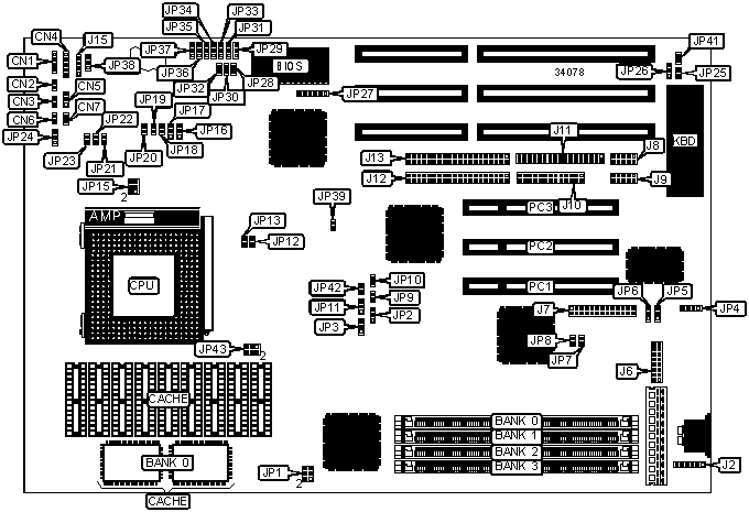
CONNECTIONS | |||
|
Purpose |
Location |
Purpose |
Location |
|
Speaker |
CN1 |
Serial port 2 |
J8 |
|
Reset switch |
CN2 |
Serial port 1 |
J9 |
|
Turbo LED |
CN3 |
Parallel port |
J10 |
|
Power LED & keylock |
CN4 |
Floppy drive interface |
J11 |
|
Turbo switch |
CN5 |
IDE interface 1 |
J12 |
|
IDE interface LED |
CN6 |
IDE interface 2 |
J13 |
|
BK LED |
CN7 |
External battery |
J15 |
|
PS/2 mouse interface |
J2 |
32-bit PCI slots |
PC1 – PC3 |
|
VGA feature connector |
J7 | ||
|
USER CONFIGURABLE SETTINGS | |||
|
Function |
Label |
Position | |
|
» |
Factory configured - do not alter |
J6 |
Unidentified |
|
» |
Factory configured - do not alter |
JP4 |
Unidentified |
|
» |
Factory configured - do not alter |
JP5 |
Unidentified |
|
» |
Factory configured - do not alter |
JP6 |
Unidentified |
|
» |
Factory configured - do not alter |
JP7 |
Unidentified |
|
» |
Factory configured - do not alter |
JP9 |
Open |
|
» |
Factory configured - do not alter |
JP15 |
Unidentified |
|
» |
CPU write select write back |
JP16 |
Pins 1 & 2 closed |
|
CPU write select write through |
JP16 |
Pins 2 & 3 closed | |
|
» |
CPU pipeline enabled |
JP17 |
Pins 2 & 3 closed |
|
CPU pipeline disabled |
JP17 |
Pins 1 & 2 closed | |
|
» |
Suspend mode disabled |
JP20 |
Open |
|
Suspend mode enabled |
JP20 |
Closed | |
|
» |
Break switch for suspend mode |
JP24 |
Pins 2 & 3 closed |
|
8042 RC enabled |
JP24 |
Pins 1 & 2 closed | |
|
» |
Monitor type select monochrome |
JP25 |
Open |
|
Monitor type select color |
JP25 |
Closed | |
|
» |
Factory configured - do not alter |
JP26 |
Unidentified |
|
» |
Factory configured - do not alter |
JP27 |
Unidentified |
|
» |
Factory configured - do not alter |
JP28 |
Unidentified |
|
» |
Factory configured - do not alter |
JP29 |
Unidentified |
|
» |
Factory configured - do not alter |
JP30 |
Unidentified |
|
» |
Factory configured - do not alter |
JP31 |
Unidentified |
|
» |
Factory configured - do not alter |
JP32 |
Unidentified |
|
» |
Factory configured - do not alter |
JP33 |
Unidentified |
|
» |
Factory configured - do not alter |
JP34 |
Unidentified |
|
» |
Factory configured - do not alter |
JP35 |
Unidentified |
|
» |
Factory configured - do not alter |
JP36 |
Unidentified |
|
» |
Factory configured - do not alter |
JP37 |
Unidentified |
|
USER CONFIGURABLE SETTINGS (CON’T) | |||
|
Function |
Label |
Position | |
|
» |
CMOS memory normal operation |
JP38 |
Pins 1 & 2 closed |
|
CMOS memory clear |
JP38 |
Pins 2 & 3 closed | |
|
» |
PCICLK speed select 1/2 CPU CLK |
JP39 |
Closed |
|
PCICLK speed select = 32MHz |
JP39 |
Open | |
|
» |
PS/2 IRQ12 enabled |
JP41 |
Closed |
|
PS/2 IRQ12 disabled |
JP41 |
Open | |
|
» |
Factory configured - do not alter |
JP42 |
Unidentified |
|
DRAM CONFIGURATION | ||||
|
Size |
Bank 0 |
Bank 1 |
Bank 2 |
Bank 3 |
|
4MB |
(1) 1M x 36 |
None |
None |
None |
|
8MB |
(1) 2M x 36 |
None |
None |
None |
|
8MB |
(1) 1M x 36 |
(1) 1M x 36 |
None |
None |
|
16MB |
(1) 4M x 36 |
None |
None |
None |
|
16MB |
(1) 2M x 36 |
(1) 2M x 36 |
None |
None |
|
16MB |
(1) 1M x 36 |
(1) 1M x 36 |
(1) 1M x 36 |
(1) 1M x 36 |
|
24MB |
(1) 1M x 36 |
(1) 1M x 36 |
(1) 2M x 36 |
(1) 2M x 36 |
|
32MB |
(1) 8M x 36 |
None |
None |
None |
|
32MB |
(1) 4M x 36 |
(1) 4M x 36 |
None |
None |
|
32MB |
(1) 2M x 36 |
(1) 2M x 36 |
(1) 2M x 36 |
(1) 2M x 36 |
|
40MB |
(1) 4M x 36 |
(1) 4M x 36 |
(1) 1M x 36 |
(1) 1M x 36 |
|
48MB |
(1) 4M x 36 |
(1) 4M x 36 |
(1) 2M x 36 |
(1) 2M x 36 |
|
64MB |
(1) 4M x 36 |
(1) 4M x 36 |
(1) 4M x 36 |
(1) 4M x 36 |
|
72MB |
(1) 8M x 36 |
(1) 8M x 36 |
(1) 1M x 36 |
(1) 1M x 36 |
|
80MB |
(1) 8M x 36 |
(1) 8M x 36 |
(1) 2M x 36 |
(1) 2M x 36 |
|
96MB |
(1) 8M x 36 |
(1) 8M x 36 |
(1) 4M x 36 |
(1) 4M x 36 |
|
128MB |
(1) 8M x 36 |
(1) 8M x 36 |
(1) 8M x 36 |
(1) 8M x 36 |
|
Note: Board accepts EDO memory. Board also accepts x 32 SIMMs. | ||||
|
DRAM VOLTAGE CONFIGURATION | ||
|
Voltage |
JP1 | |
| » |
Mixed mode |
Pins 3 & 5, 4 & 6 closed |
|
3.3v |
Pins 1 & 3, 2 & 4 closed | |
|
CACHE CONFIGURATION | |||
|
Size |
Bank 0 |
Bank 1 |
TAG |
|
256KB (A) |
None |
(8) 32K x 8 |
(1) 8K x 8 |
|
256KB (B) |
(2) 32K x 32 |
None |
Unidentified |
|
512KB (A) |
None |
(8) 64K x 8 |
(1) 16K x 8 (Windbond) |
|
512KB (B) |
None |
(8) 64K x 8 |
(1) 16K/32K x 8 (Aster) |
|
1MB |
None |
(8) 128K x 8 |
(1) 32K x 8 |
|
Note: The location of bank 1 & TAG are unidentified. | |||
|
CACHE JUMPER CONFIGURATION | |||
|
Size |
JP3 |
JP11 |
JP42 |
|
256KB (A) |
Pins 1 & 2 closed |
Pins 1 & 2 closed |
Open |
|
256KB (B) |
Pins 1 & 2 closed |
Pins 1 & 2 closed |
Open |
|
512KB (A) |
Pins 2 & 3 closed |
Open |
Closed |
|
512KB (B) |
Pins 2 & 3 closed |
Pins 1 & 2 closed |
Open |
|
1MB |
Pins 2 & 3 closed |
Pins 2 & 3 closed |
Open |
|
CPU SPEED SELECTION | ||||||
|
CPU speed |
Clock speed |
Multiplier |
JP12 |
JP13 |
JP18 |
JP19 |
|
75MHz |
50MHz |
1.5x |
Closed |
Closed |
Open |
Open |
|
90MHz |
60MHz |
1.5x |
Closed |
Open |
Open |
Open |
|
100MHz |
66MHz |
1.5x |
Open |
Closed |
Open |
Open |
|
120MHz |
60MHz |
2x |
Closed |
Open |
Open |
Closed |
|
133MHz |
66MHz |
2x |
Open |
Closed |
Open |
Closed |
|
150MHz |
60MHz |
2.5x |
Closed |
Open |
Closed |
Closed |
|
166MHz |
66MHz |
2.5x |
Open |
Closed |
Closed |
Closed |
|
CPU VOLTAGE SELECTION | ||||
|
Voltage |
JP21 |
JP22 |
JP23 | |
|
3.3v |
Closed |
Open |
Open | |
| » |
3.45v |
Open |
Closed |
Open |
|
3.6v |
Open |
Open |
Closed | |
|
VGA SELECTION | ||||
|
Setting |
JP2 |
JP8 |
JP10 | |
| » |
Onboard VGA |
Pins 1 & 2 closed |
Closed |
Closed |
|
External VGA card |
Pins 2 & 3 closed |
Open |
Open | |