MORSE TECHNOLOGIES, INC.
SHUTTLE 386SX
|
Processor |
80386SX |
|
Processor Speed |
16MHz |
|
Chip Set |
Intel |
|
Max. Onboard DRAM |
8MB |
|
Cache |
None |
|
BIOS |
AMI |
|
Dimensions |
331mm x 220mm |
|
I/O Options |
None |
|
NPU Options |
80387SX |
|
CONNECTIONS | |||
|
Purpose |
Location |
Purpose |
Location |
|
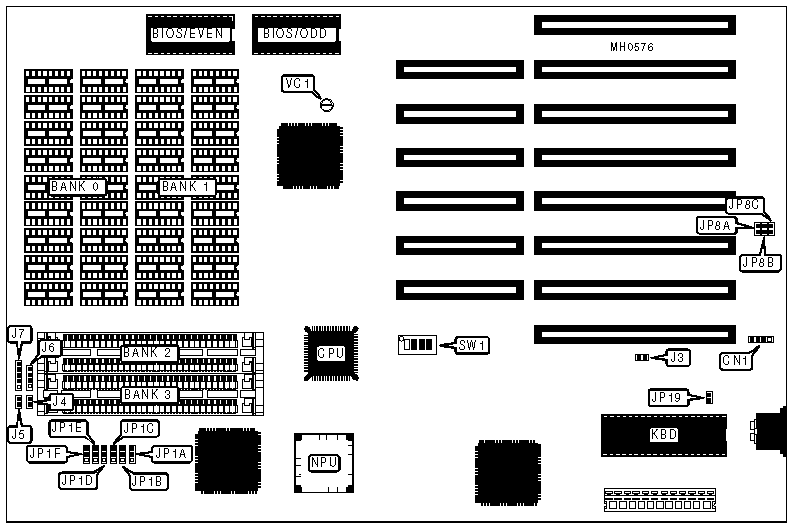
External battery |
CN1 |
Turbo switch |
J5 |
|
Reset switch |
J3 |
Speaker |
J6 |
|
Turbo LED |
J4 |
Power LED & keylock |
J7 |
|
USER CONFIGURABLE SETTINGS | |||
|
Function |
Jumper/Switch |
Position | |
| » |
Turbo mode output signal select pin 23 |
JP8A |
Closed |
|
Turbo mode output signal select pin 30 |
JP8B |
Closed | |
|
Turbo mode output signal select pin 32 |
JP8C |
Closed | |
| » |
Battery enabled |
JP19 |
Closed |
|
Battery disabled |
JP19 |
Open | |
| » |
BIOS type select 27256 |
SW1/1 |
Off |
|
BIOS type select 27512 |
SW1/1 |
On | |
| » |
Monitor type select color |
SW1/2 |
On |
|
Monitor type select monochrome |
SW1/2 |
Off | |
| » |
CGA fine color tuning |
VC1 |
Variable |
|
DRAM CONFIGURATION | ||||
|
Size |
Bank 0 |
Bank 1 |
Bank 2 |
Bank 3 |
|
512KB |
(18) 41256 |
NONE |
NONE |
NONE |
|
512KB |
NONE |
NONE |
(2) 256K x 9 |
NONE |
|
1MB |
(18) 41256 |
(18) 41256 |
NONE |
NONE |
|
1MB |
NONE |
NONE |
(2) 256K x 9 |
(2) 256K x 9 |
|
2MB |
(18) 41256 |
(18) 41256 |
(2) 256K x 9 |
(2) 256K x 9 |
|
2MB |
(18) 411000 |
NONE |
NONE |
NONE |
|
2MB |
NONE |
NONE |
(2) 1M x 9 |
NONE |
|
4MB |
(18) 411000 |
(18) 411000 |
NONE |
NONE |
|
4MB |
NONE |
NONE |
(2) 1M x 9 |
(2) 1M x 9 |
|
8MB |
(18) 411000 |
(18) 411000 |
(2) 1M x 9 |
(2) 1M x 9 |
|
DRAM JUMPER CONFIGURATION | ||||||
|
Size |
JP1A |
JP1B |
JP1C |
JP1D |
JP1E |
JP1F |
|
512KB |
1 & 2 |
1 & 2 |
1 & 2 |
1 & 2 |
1 & 2 |
1 & 2 |
|
512KB |
1 & 2 |
1 & 2 |
1 & 2 |
1 & 2 |
1 & 2 |
1 & 2 |
|
1MB |
1 & 2 |
1 & 2 |
1 & 2 |
1 & 2 |
1 & 2 |
1 & 2 |
|
1MB |
1 & 2 |
1 & 2 |
1 & 2 |
1 & 2 |
1 & 2 |
1 & 2 |
|
2MB |
2 & 3 |
2 & 3 |
2 & 3 |
2 & 3 |
2 & 3 |
2 & 3 |
|
2MB |
1 & 2 |
1 & 2 |
1 & 2 |
1 & 2 |
1 & 2 |
1 & 2 |
|
2MB |
1 & 2 |
1 & 2 |
1 & 2 |
1 & 2 |
1 & 2 |
1 & 2 |
|
4MB |
1 & 2 |
1 & 2 |
1 & 2 |
1 & 2 |
1 & 2 |
1 & 2 |
|
4MB |
1 & 2 |
1 & 2 |
1 & 2 |
1 & 2 |
1 & 2 |
1 & 2 |
|
8MB |
2 & 3 |
2 & 3 |
2 & 3 |
2 & 3 |
2 & 3 |
2 & 3 |
|
Note:Pins designated should be in the closed position. | ||||||
|
DRAM WAIT STATE CONFIGURATION | ||
|
Setting |
SW1/3 |
SW1/4 |
|
1 wait state at multiple page mode |
On |
Off |
|
1 wait state at 1 page mode |
Off |
Off |
|
2 wait states at 1 page mode |
Off |
On |
|
3 wait states at 1 page mode |
On |
On |