NORTHGATE COMPUTER SYSTEMS, INC.
ELEGANCE PENTIUM 90
|
Processor |
Pentium |
|
Processor Speed |
60/66/75/90/100MHz |
|
Chip Set |
OPTI |
|
Max. Onboard DRAM |
128MB |
|
Cache |
256/1024KB |
|
BIOS |
AMI/Phoenix |
|
Dimensions |
330mm x 218mm |
|
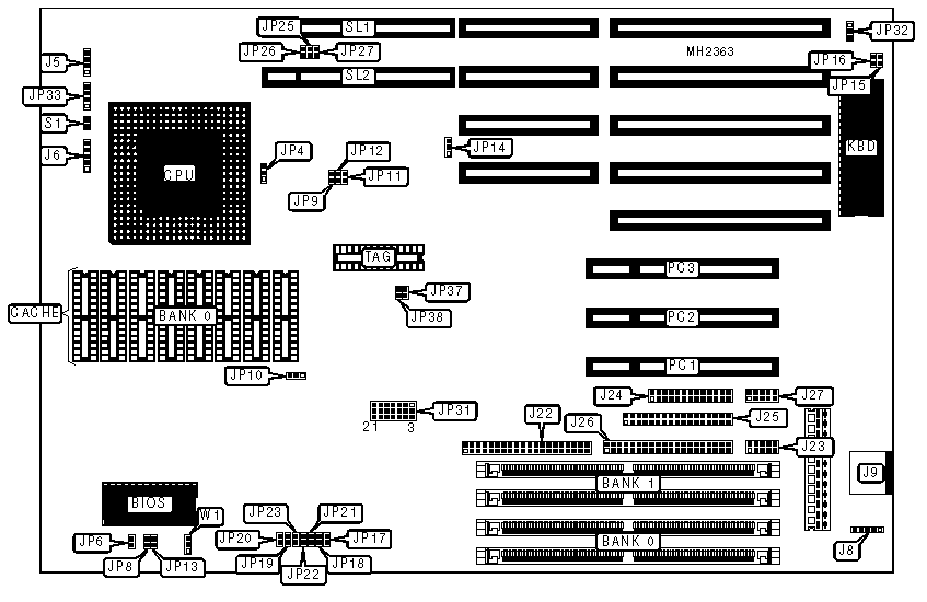
I/O Options |
32-bit VESA local bus slots (2), 32-bit PCI bus slots (3), floppy drive interface, IDE interfaces (2), parallel port, PS/2 mouse port, serial ports (2) |
|
NPU Options |
None |
|
CONNECTIONS | |||
|
Purpose |
Location |
Purpose |
Location |
|
Speaker |
J5 |
IDE interface |
J26 |
|
Power LED & keylock |
J6 |
Serial port 2 |
J27 |
|
Keyboard connector |
J8 |
Turbo LED |
JP33 (pins 1 - 2) |
|
PS/2 mouse port |
J9 |
IDE interface LED |
JP33 (pins 3 - 4) |
|
IDE interface |
J22 |
32-bit PCI bus slots |
PC1 - PC3 |
|
Serial port 1 |
J23 |
Reset switch |
S1 |
|
Parallel port |
J24 |
32-bit VESA local bus slots |
SL1 & SL2 |
|
Floppy drive interface |
J25 | ||
|
USER CONFIGURABLE SETTINGS | |||
|
Function |
Jumper |
Position | |
|
» |
Factory configured - do not alter |
JP1 |
Open |
|
» |
Factory configured - do not alter |
JP2 |
Open |
|
» |
Factory configured - do not alter |
JP3 |
Open |
|
» |
Factory configured - do not alter |
JP4 |
pins 2 & 3 closed |
|
» |
Factory configured - do not alter |
JP6 |
Open |
|
» |
Factory configured - do not alter |
JP8 |
Open |
|
» |
Factory configured - do not alter |
JP10 |
pins 2 & 3 closed |
|
» |
Factory configured - do not alter |
JP13 |
Open |
|
» |
CMOS memory normal operation |
JP14 |
pins 1 & 2 closed |
|
CMOS memory clear |
JP14 |
pins 2 & 3 closed | |
|
» |
Monitor type select color |
JP15 |
Closed |
|
Monitor type select monochrome |
JP15 |
Open | |
|
» |
Factory configured - do not alter |
JP16 |
Open |
|
» |
I/O recovery delay delay enabled |
JP19 |
Closed |
|
I/O recovery delay delay disabled |
JP19 |
Open | |
|
» |
LDEV# timing select end of first T2 |
JP20 |
Open |
|
LDEV# timing select end of second T2 |
JP20 |
Closed | |
|
» |
Factory configured - do not alter |
JP21 |
Open |
|
» |
Factory configured - do not alter |
JP22 |
Open |
|
» |
Main board select SQ545 |
JP23 |
Closed |
|
Main board select SQ503 |
JP23 |
Open | |
|
» |
Factory configured - do not alter |
JP26 |
Closed |
|
» |
Factory configured - do not alter |
JP28 |
Open |
|
» |
Factory configured - do not alter |
JP29 |
pins 1 & 2 closed |
|
» |
Factory configured - do not alter |
JP30 |
Closed |
|
» |
Port 3F7 mode select VESA |
JP31 |
pins 8 & 9 closed |
|
Port 3F7 mode select ISA |
JP31 |
pins 7 & 8 closed | |
|
» |
IDE port address select primary |
JP31 |
pins 10 & 11 closed |
|
IDE port address select secondary |
JP31 |
pins 11 & 12 closed | |
|
» |
VESA IDE enabled |
JP31 |
pins 19 & 20 closed |
|
VESA IDE disabled |
JP31 |
pins 20 & 21 closed | |
|
» |
Parallel port IRQ select IRQ7 |
JP32 |
pins 1 & 2 closed |
|
Parallel port IRQ select IRQ5 |
JP32 |
pins 2 & 3 closed | |
|
» |
Flash EPROM select normal operation |
W1 |
pins 1 & 2 closed |
|
Flash EPROM select flash programming |
W1 |
pins 2 & 3 closed | |
|
Note: The location of the following jumpers are unidentified: JP1, JP2, JP3, JP28, JP29, & JP30. | |||
|
DRAM CONFIGURATION | ||
|
Size |
Bank 0 |
Bank 1 |
|
2MB |
(2) 256K x 36 |
NONE |
|
4MB |
(2) 256K x 36 |
(2) 256K x 36 |
|
4MB |
(2) 512K x 36 |
NONE |
|
6MB |
(2) 256K x 36 |
(2) 512K x 36 |
|
8MB |
(2) 512K x 36 |
(2) 512K x 36 |
|
10MB |
(2) 1M x 36 |
(2) 256K x 36 |
|
12MB |
(2) 1M x 36 |
(2) 512K x 36 |
|
16MB |
(2) 1M x 36 |
(2) 1M x 36 |
|
16MB |
(2) 2M x 36 |
NONE |
|
18MB |
(2) 256K x 36 |
(2) 2M x 36 |
|
20MB |
(2) 512K x 36 |
(2) 2M x 36 |
|
24MB |
(2) 1M x 36 |
(2) 2M x 36 |
|
32MB |
(2) 2M x 36 |
(2) 2M x 36 |
|
32MB |
(2) 4M x 36 |
NONE |
|
34MB |
(2) 256K x 36 |
(2) 4M x 36 |
|
36MB |
(2) 512K x 36 |
(2) 4M x 36 |
|
40MB |
(2) 1M x 36 |
(2) 4M x 36 |
|
48MB |
(2) 2M x 36 |
(2) 4M x 36 |
|
64MB |
(2) 4M x 36 |
(2) 4M x 36 |
|
64MB |
(2) 8M x 36 |
NONE |
|
66MB |
(2) 256K x 36 |
(2) 8M x 36 |
|
68MB |
(2) 512K x 36 |
(2) 8M x 36 |
|
72MB |
(2) 1M x 36 |
(2) 8M x 36 |
|
80MB |
(2) 2M x 36 |
(2) 8M x 36 |
|
96MB |
(2) 4M x 36 |
(2) 8M x 36 |
|
128MB |
(2) 8M x 36 |
(2) 8M x 36 |
|
CACHE CONFIGURATION | ||
|
Size |
Bank 0 |
TAG |
|
256KB |
(8) 32K x 8 |
(1) 32K x 8 |
|
1MB |
(8) 128K x 8 |
(1) 32K x 8 |
|
CACHE JUMPER CONFIGURATION | ||
|
Size |
JP37 |
JP38 |
|
256KB |
Open |
Open |
|
1MB |
Closed |
Closed |
|
CPU SPEED CONFIGURATION | |||
|
Speed |
JP9 |
JP11 |
JP12 |
|
50MHz |
Open |
Closed |
Closed |
|
60MHz |
Closed |
Open |
Closed |
|
66MHz |
Open |
Closed |
Open |
|
75MHz |
Open |
Closed |
Closed |
|
90MHz |
Closed |
Open |
Closed |
|
100MHz |
Open |
Closed |
Open |
|
VESA CLOCK SPEED CONFIGURATION | ||
|
Speed |
JP31 | |
| » |
33MHz |
pins 2 & 3, 4 & 5 closed |
|
25MHz |
pins 1 & 2, 4 & 5 closed | |
|
40MHz |
pins 1 & 2, 5 & 6 closed | |
|
50MHz |
pins 2 & 3, 5 & 6 closed | |
|
VESA CYCLE TIME CONFIGURATION | ||
|
Cycle time |
JP31 | |
| » |
> = 480ns |
pins 14 & 15, 17 & 18 closed |
|
> = 200ns |
pins 13 & 14, 16 & 17 closed | |
|
> = 240ns |
pins 14 & 15, 16 & 17 closed | |
|
> = 383ns |
pins 13 & 14, 17 & 18 closed | |
|
BUS SPEED CONFIGURATION | |
|
CPU speed |
JP25 |
|
<= 33MHz |
Open |
|
> 33MHz |
Closed |
|
BUS SPEED CONFIGURATION | |||
|
Setting |
JP17 |
JP18 | |
| » |
LCLK/4 |
Open |
Closed |
|
LCLK/2 |
Open |
Open | |
|
LCLK/3 |
Closed |
Open | |
|
LCLK/5 |
Closed |
Closed | |