OLIVETTI
M6-420/440/450/460/ (BA200X)
|
Processor |
80486SX/80487SX/80486DX/80486DX2/P24T |
|
Processor Speed |
25/33/50(internal)/66(internal)MHz |
|
Chip Set |
Unidentified |
|
Maximum Onboard Memory |
100MB |
|
Cache |
256KB |
|
BIOS |
Unidentified |
|
Dimensions |
330mm x 218mm |
|
I/O Options |
Floppy drive interface, IDE interface, parallel port, PS/2 mouse port, serial ports (2), VGA feature connector, VGA port, cache slot, riser slot, audio board connector |
|
NPU Options |
None |
|
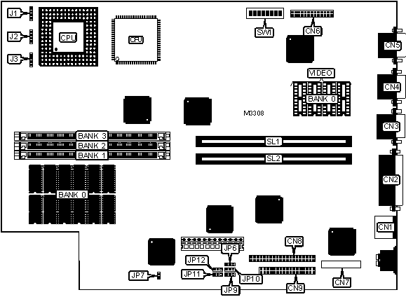
CONNECTIONS | |||
|
Function |
Label |
Function |
Label |
|
PS/2 mouse port |
CN1 |
Floppy drive interface |
CN9 |
|
Parallel port |
CN2 |
Chassis fan power |
J1 |
|
Serial port 1 |
CN3 |
Speaker |
J2 |
|
Serial port 2 |
CN4 |
External battery |
J3 |
|
VGA port |
CN5 |
Reset switch |
JP7 |
|
VGA feature connector |
CN6 |
Cache slot |
SL1 |
|
Audio board connector |
CN7 |
Riser slot |
SL2 |
|
IDE interface |
CN8 | ||
|
Note: The location of pin 1 on the connectors is unidentified. | |||
|
USER CONFIGURABLE SETTINGS | |||
|
Setting |
Label |
Position | |
|
» |
CMOS memory normal operation |
JP6 |
Open |
|
CMOS memory clear |
JP6 |
Pins 2 & 3 closed | |
|
System normal operation |
JP7 |
Open | |
|
System reset |
JP7 |
Closed | |
|
» |
87311/12 address select 398 - 399 |
SW1/1 |
Off |
|
87311/12 address select 26E - 26F |
SW1/1 |
On | |
|
» |
Setup access enabled |
SW1/2 |
Off |
|
Setup access disabled |
SW1/2 |
On | |
|
» |
Bootstrap from serial port enabled |
SW1/3 |
Off |
|
Bootstrap from serial port disabled |
SW1/3 |
On | |
|
» |
Flash BIOS write disabled |
SW1/4 |
Off |
|
Flash BIOS write enabled |
SW1/4 |
On | |
|
» |
Floppy drive write enabled |
SW1/5 |
Off |
|
Floppy drive write disabled |
SW1/5 |
On | |
|
» |
RAMDAC write enabled |
SW1/6 |
Off |
|
RAMDAC write disabled |
SW1/6 |
On | |
|
On board video enabled |
SW1/7 |
Off | |
|
On board video disabled |
SW1/7 |
On | |
|
Note: The location of pin 1 on SW1 is unidentified. | |||
|
DRAM | ||||
|
Size |
Bank 0 |
Bank 1 |
Bank 2 |
Bank 3 |
|
4MB |
4MB |
None |
None |
None |
|
8MB |
4MB |
(1) 1M x 36 |
None |
None |
|
12MB |
4MB |
(1) 2M x 36 |
None |
None |
|
12MB |
4MB |
(1) 1M x 36 |
(1) 1M x 36 |
None |
|
16MB |
4MB |
(1) 2M x 36 |
(1) 1M x 36 |
None |
|
16MB |
4MB |
(1) 1M x 36 |
(1) 1M x 36 |
(1) 1M x 36 |
|
16MB |
4MB |
(1) 1M x 36 |
(1) 2M x 36 |
None |
|
20MB |
4MB |
(1) 4M x 36 |
None |
None |
|
20MB |
4MB |
(1) 2M x 36 |
(1) 1M x 36 |
(1) 1M x 36 |
|
DRAM (CON’T) | ||||
|
Size |
Bank 0 |
Bank 1 |
Bank 2 |
Bank 3 |
|
20MB |
4MB |
(1) 2M x 36 |
(1) 2M x 36 |
None |
|
24MB |
4MB |
(1) 4M x 36 |
(1) 1M x 36 |
None |
|
24MB |
4MB |
(1) 1M x 36 |
(1) 2M x 36 |
(1) 2M x 36 |
|
24MB |
4MB |
(1) 1M x 36 |
(1) 4M x 36 |
None |
|
28MB |
4MB |
(1) 4M x 36 |
(1) 1M x 36 |
(1) 1M x 36 |
|
28MB |
4MB |
(1) 4M x 36 |
(1) 2M x 36 |
None |
|
28MB |
4MB |
(1) 2M x 36 |
(1) 2M x 36 |
(1) 2M x 36 |
|
28MB |
4MB |
(1) 2M x 36 |
(1) 4M x 36 |
None |
|
36MB |
4MB |
(1) 8M x 36 |
None |
None |
|
36MB |
4MB |
(1) 4M x 36 |
(1) 2M x 36 |
(1) 2M x 36 |
|
36MB |
4MB |
(1) 4M x 36 |
(1) 4M x 36 |
None |
|
40MB |
4MB |
(1) 8M x 36 |
(1) 1M x 36 |
None |
|
40MB |
4MB |
(1) 1M x 36 |
(1) 4M x 36 |
(1) 4M x 36 |
|
40MB |
4MB |
(1) 1M x 36 |
(1) 8M x 36 |
None |
|
44MB |
4MB |
(1) 8M x 36 |
(1) 1M x 36 |
(1) 1M x 36 |
|
44MB |
4MB |
(1) 8M x 36 |
(1) 2M x 36 |
None |
|
44MB |
4MB |
(1) 2M x 36 |
(1) 4M x 36 |
(1) 4M x 36 |
|
44MB |
4MB |
(1) 2M x 36 |
(1) 8M x 36 |
None |
|
52MB |
4MB |
(1) 8M x 36 |
(1) 2M x 36 |
(1) 2M x 36 |
|
52MB |
4MB |
(1) 8M x 36 |
(1) 4M x 36 |
None |
|
52MB |
4MB |
(1) 4M x 36 |
(1) 4M x 36 |
(1) 4M x 36 |
|
52MB |
4MB |
(1) 4M x 36 |
(1) 8M x 36 |
None |
|
70MB |
4MB |
(1) 8M x 36 |
(1) 4M x 36 |
(1) 4M x 36 |
|
70MB |
4MB |
(1) 8M x 36 |
(1) 8M x 36 |
None |
|
72MB |
4MB |
(1) 1M x 36 |
(1) 8M x 36 |
(1) 8M x 36 |
|
76MB |
4MB |
(1) 2M x 36 |
(1) 8M x 36 |
(1) 8M x 36 |
|
84MB |
4MB |
(1) 4M x 36 |
(1) 8M x 36 |
(1) 8M x 36 |
|
100MB |
4MB |
(1) 8M x 36 |
(1) 8M x 36 |
(1) 8M x 36 |
|
Note: Bank 0 is factory installed and is not configurable. | ||||
|
CACHE SIZE | |
|
Size |
SL1 |
|
256KB |
Installed |
|
CPU SPEED | |
|
Setting |
SW1/8 |
|
25MHz |
Off |
|
33MHz |
On |
|
50iMHz |
Off |
|
66iMHz |
On |
|
DMA CHANNEL | ||||
|
Setting |
JP9 |
JP10 |
JP11 |
JP12 |
|
DMA0 |
Pins 1 & 2 closed |
N/A |
Pins 1 & 2 closed |
N/A |
|
DMA1 |
N/A |
Pins 1 & 2 closed |
N/A |
Pins 1 & 2 closed |
|
DMA5 |
Pins 2 & 3 closed |
N/A |
Pins 2 & 3 closed |
N/A |
|
VIDEO MEMORY | |
|
Size |
Bank 0 |
|
None |
None |
|
1MB |
(4) 256K x 8 |