MOTOROLA, INC.
PV5000
|
Device Type |
Single board computer |
|
Processor |
AM K6/Pentium/Pentium MMX |
|
Processor Speed |
133/166/200/233/266/300MHz |
|
Chip Set |
Unidentified |
|
Video Chip Set |
Unidentified |
|
Maximum Onboard Memory |
256MB (EDO supported) |
|
Maximum Video Memory |
Unidentified |
|
Cache |
256/512KB |
|
BIOS |
AMI |
|
Dimensions |
338mm x 122mm |
|
I/O Options |
Ethernet 10BaseT connector, floppy drive interface, IDE interfaces (2), SCSI interface, parallel port, PS/2 mouse port, serial ports (2), VGA port, cache slot, USB connectors (2) |
|
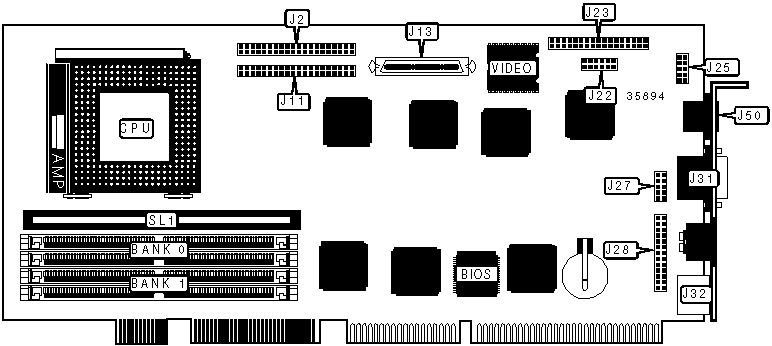
CONNECTIONS | |||
|
Purpose |
Location |
Purpose |
Location |
|
Debug connector |
J1 |
USB connector 2 |
J24 |
|
IDE interface 1 |
J2 |
Serial port 2 |
J25 |
|
EPLD ISP connector |
J3 |
Serial port 1 |
J27 |
|
IDE interface 2 |
J11 |
Parallel port |
J28 |
|
SCSI interface |
J13 |
VGA port |
J31 |
|
Alarm connector |
J17 |
PS/2 mouse port |
J32 |
|
Reset switch |
J19 |
FPGA ISP connector |
J34 |
|
Speaker |
J20 |
USB connector 1 |
J35 |
|
IDE interface LED |
J21 |
Ethernet 10BaseT connector |
J50 |
|
Temperature sensor |
J22 |
Cache slot |
SL1 |
|
Floppy drive interface |
J23 | ||
|
Note: The location of J1, J3, J17, J19, J20, J21, J24, J34 & J35 are unidentified. | |||
|
SIMM CONFIGURATION | ||
|
Size |
Bank 0 |
Bank 1 |
|
8MB |
(2) 1M x 36 |
None |
|
16MB |
(2) 2M x 36 |
None |
|
16MB |
(2) 1M x 36 |
(2) 1M x 36 |
|
24MB |
(2) 2M x 36 |
(2) 1M x 36 |
|
32MB |
(2) 4M x 36 |
None |
|
32MB |
(2) 2M x 36 |
(2) 2M x 36 |
|
40MB |
(2) 4M x 36 |
(2) 1M x 36 |
|
48MB |
(2) 4M x 36 |
(2) 2M x 36 |
|
64MB |
(2) 8M x 36 |
None |
|
64MB |
(2) 4M x 36 |
(2) 4M x 36 |
|
72MB |
(2) 8M x 36 |
(2) 1M x 36 |
|
80MB |
(2) 8M x 36 |
(2) 2M x 36 |
|
96MB |
(2) 8M x 36 |
(2) 4M x 36 |
|
128MB |
(2) 8M x 36 |
(2) 8M x 36 |
|
128MB |
(2) 16M x 36 |
None |
|
136MB |
(2) 16M x 36 |
(2) 1M x 36 |
|
144MB |
(2) 16M x 36 |
(2) 2M x 36 |
|
160MB |
(2) 16M x 36 |
(2) 4M x 36 |
|
192MB |
(2) 16M x 36 |
(2) 8M x 36 |
|
256MB |
(2) 16M x 36 |
(2) 16M x 36 |
|
Note: Board accepts EDO memory. | ||
|
CACHE CONFIGURATION |
|
Note: The location of the cache is unidentified. |
|
VIDEO MEMORY CONFIGURATION |
|
Note: The size & location of the video memory is unidentified. |
|
CPU SPEED SELECTION (AM K6) | ||||||
|
CPU speed |
Clock speed |
Multiplier |
J10 |
J14 |
J15 |
J29 |
|
166MHz |
66MHz |
2.5x |
2 & 3 |
1 & 2 |
1 & 2 |
2 & 3 |
|
200MHz |
66MHz |
3x |
2 & 3 |
1 & 2 |
2 & 3 |
2 & 3 |
|
233MHz |
66MHz |
3.5x |
2 & 3 |
2 & 3 |
2 & 3 |
2 & 3 |
|
266MHz |
66MHz |
4x |
2 & 3 |
2 & 3 |
1 & 2 |
1 & 2 |
|
300MHz |
66MHz |
4.5x |
2 & 3 |
1 & 2 |
1 & 2 |
1 & 2 |
|
Note: Pins designated should be in the closed position. The location of the jumpers is unidentified. | ||||||
|
CPU SPEED SELECTION (INTEL) | ||||||
|
CPU speed |
Clock speed |
Multiplier |
J10 |
J14 |
J15 |
J29 |
|
133MHz |
66MHz |
2x |
2 & 3 |
2 & 3 |
1 & 2 |
2 & 3 |
|
166MHz |
66MHz |
2.5x |
2 & 3 |
1 & 2 |
1 & 2 |
2 & 3 |
|
200MHz |
66MHz |
3x |
2 & 3 |
1 & 2 |
2 & 3 |
2 & 3 |
|
Note: Pins designated should be in the closed position. The location of the jumpers is unidentified. | ||||||
|
CPU SPEED SELECTION (INTEL MMX) | ||||||
|
CPU speed |
Clock speed |
Multiplier |
J10 |
J14 |
J15 |
J29 |
|
166MHz |
66MHz |
2.5x |
2 & 3 |
1 & 2 |
1 & 2 |
2 & 3 |
|
200MHz |
66MHz |
3x |
2 & 3 |
1 & 2 |
2 & 3 |
2 & 3 |
|
233MHz |
66MHz |
3.5x |
2 & 3 |
2 & 3 |
2 & 3 |
2 & 3 |
|
Note: Pins designated should be in the closed position. The location of the jumpers is unidentified. | ||||||