RELIALOGIC CORPORATION PRIVATE, LTD.
SI54A
|
Processor |
Pentium |
|
Processor Speed |
75/90/100MHz |
|
Chip Set |
SIS |
|
Max. Onboard DRAM |
128MB |
|
Cache |
256/512/1024KB |
|
BIOS |
Award |
|
Dimensions |
330mm x 218mm |
|
I/O Options |
32-bit PCI slots (4), floppy drive interface, IDE interfaces (2), parallel port, serial ports (2) |
|
NPU Options |
None |
|
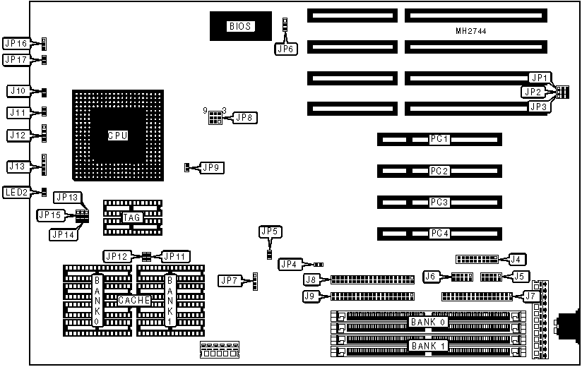
CONNECTIONS | |||
|
Purpose |
Location |
Purpose |
Location |
|
Parallel port |
J4 |
Reset switch |
J11 |
|
Serial port 1 |
J5 |
Speaker |
J12 |
|
Serial port 2 |
J6 |
Power LED & keylock |
J13 |
|
Floppy drive interface |
J7 |
Turbo LED |
LED1 |
|
IDE interface (secondary) |
J8 |
IDE interface LED |
LED2 |
|
IDE interface (primary) |
J9 |
32-bit PCI slots |
PCI - PC4 |
|
Turbo switch |
J10 | ||
|
Note: The location of LED1 is unidentified. | |||
|
USER CONFIGURABLE SETTINGS | |||
|
Function |
Jumper |
Position | |
|
» |
On board I/O enabled |
JP3 |
pins 1 & 2 closed |
|
On board I/O disabled |
JP3 |
pins 2 & 3 closed | |
|
» |
IDE interface enabled |
JP4 |
Open |
|
IDE interface disabled |
JP4 |
Closed | |
|
» |
Parity check enabled |
JP5 |
Closed |
|
Parity check disabled |
JP5 |
Open | |
|
» |
Factory configured - do not alter |
JP9 |
N/A |
|
» |
Cache invalidation select always invalidated |
JP13 |
pins 1 & 2 closed |
|
Cache invalidation select writes to invalidated |
JP13 |
pins 2 & 3 closed | |
|
» |
Cache write select write back |
JP14 |
pins 1 & 2 closed |
|
Cache write select write through |
JP14 |
pins 2 & 3 closed | |
|
» |
Factory configured - do not alter |
JP15 |
N/A |
|
» |
Factory configured - do not alter |
JP16 |
N/A |
|
» |
Factory configured - do not alter |
JP17 |
N/A |
|
DRAM CONFIGURATION | ||
|
Size |
Bank 0 |
Bank 1 |
|
2MB |
(2) 256K x 36 |
NONE |
|
4MB |
(2) 256K x 36 |
(2) 256K x 36 |
|
4MB |
(2) 512K x 36 |
NONE |
|
8MB |
(2) 512K x 36 |
(2) 512K x 36 |
|
8MB |
(2) 1M x 36 |
NONE |
|
16MB |
(2) 1M x 36 |
(2) 1M x 36 |
|
16MB |
(2) 2M x 36 |
NONE |
|
32MB |
(2) 2M x 36 |
(2) 2M x 36 |
|
36MB |
(2) 512K x 36 |
(2) 4M x 36 |
|
40MB |
(2) 1M x 36 |
(2) 4M x 36 |
|
48MB |
(2) 2M x 36 |
(2) 4M x 36 |
|
64MB |
(2) 4M x 36 |
(2) 4M x 36 |
|
64MB |
(2) 8M x 36 |
NONE |
|
128MB |
(2) 8M x 36 |
(2) 8M x 36 |
|
128MB |
(2) 16M x 36 |
NONE |
|
DRAM JUMPER CONFIGURATION | |
|
Type |
JP7 |
|
Single side SIMMs only |
pins 2 & 3 closed |
|
Bank 0 = single side SIMMs & Bank 1 = double side SIMMs |
pins 1 & 2, 3 & 4 closed |
|
CACHE CONFIGURATION | |||
|
Size |
Bank 0 |
Bank 1 |
TAG |
|
256KB |
(4) 32K x 8 |
(4) 32K x 8 |
(2) 32K x 8 |
|
512KB |
(4) 64K x 8 |
(4) 64K x 8 |
(2) 32K x 8 |
|
1MB |
(4) 128K x 8 |
(4) 128K x 8 |
(2) 32K x 8 |
|
CACHE JUMPER CONFIGURATION | ||
|
Size |
JP11 |
JP12 |
|
256KB |
Open |
Open |
|
512KB |
Closed |
Closed |
|
1MB |
Closed |
Closed |
|
CPU SPEED CONFIGURATION | |
|
Speed |
JP8 |
|
75MHz |
pins 2 & 3, 5 & 6, 7 & 8 closed |
|
90MHz |
pins 2 & 3, 4 & 5, 8 & 9 closed |
|
100MHz |
pins 1 & 2, 5 & 6, 7 & 8 closed |
|
BIOS CONFIGURATION | |
|
Type |
JP6 |
|
EPROM |
pins 1 & 2 closed |
|
Flash 5v |
pins 1 & 2 closed |
|
Flash 12v |
pins 2 & 3 closed |
|
DACK/DRQ CONFIGURATION | ||
|
DACK/DRQ |
JP1 |
JP2 |
|
DACK1/DRQ1 |
pins 1 & 2 closed |
pins 2 & 3 closed |
|
DACK3/DRQ3 |
pins 2 & 3 closed |
pins 1 & 2 closed |