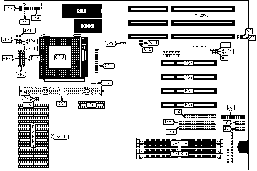
TMC RESEARCH CORPORATION
PCI54PV4 (VER. 2.10)
|
Processor |
CX M1/AMD K5/Pentium |
|
Processor Speed |
75/90/100/120/133/150/166/180/200MHz |
|
Chip Set |
OPTI |
|
Max. Onboard DRAM |
128MB |
|
Cache |
256/512/1024KB |
|
BIOS |
Unidentified |
|
Dimensions |
330mm x 218mm |
|
I/O Options |
Parallel port, serial ports (2), 32-bit PCI slots (4), green PC connector, floppy drive interface, IDE interfaces (2) |
|
NPU Options |
None |
|
CONNECTIONS | |||
|
Purpose |
Location |
Purpose |
Location |
|
Voltage regulator module |
CN1 |
Green PC connector |
J16 |
|
Serial port 1 |
J4 |
Speaker |
J14 pins 1 - 5 |
|
Serial port 2 |
J5 |
Turbo switch |
J14 pins 7 & 17 |
|
Parallel port |
J8 |
Reset switch |
J14 pins 8 & 18 |
|
Floppy drive interface |
J9 |
IDE interface LED |
J14 pins 10 & 20 |
|
External battery |
J10 |
Power LED & keylock |
J14 pins 11 - 15 |
|
IDE interface 1 |
J11 |
32-bit PCI slots |
PC1 - PC4 |
|
IDE interface 2 |
J12 | ||
|
USER CONFIGURABLE SETTINGS | |||
|
Function |
Jumper |
Position | |
|
» |
Factory configured - do not alter |
J15 |
N/A |
|
» |
CMOS memory normal operation |
JP1 |
pins 2 & 3 closed |
|
CMOS memory clear |
JP1 |
pins 1 & 2 closed | |
|
» |
Flash BIOS voltage select 12v |
JP3 |
pins 1 & 2 closed |
|
Flash BIOS voltage select 5v |
JP3 |
pins 2 & 3 closed | |
|
» |
Password normal operation |
JP9 |
Open |
|
Password clear |
JP9 |
Closed | |
|
» |
BIOS setup normal operation |
JP11 |
Open |
|
BIOS setup access denied |
JP11 |
Closed | |
|
» |
Factory configured - do not alter |
W4 |
N/A |
|
DRAM CONFIGURATION | ||
|
Size |
Bank 0 |
Bank 1 |
|
8MB |
(2) 1M x 36 |
NONE |
|
16MB |
(2) 2M x 36 |
NONE |
|
16MB |
(2) 1M x 36 |
(2) 1M x 36 |
|
24MB |
(2) 1M x 36 |
(2) 2M x 36 |
|
32MB |
(2) 4M x 36 |
NONE |
|
32MB |
(2) 2M x 36 |
(2) 2M x 36 |
|
40MB |
(2) 1M x 36 |
(2) 4M x 36 |
|
48MB |
(2) 2M x 36 |
(2) 4M x 36 |
|
64MB |
(2) 8M x 36 |
NONE |
|
64MB |
(2) 4M x 36 |
(2) 4M x 36 |
|
72MB |
(2) 1M x 36 |
(2) 8M x 36 |
|
80MB |
(2) 2M x 36 |
(2) 8M x 36 |
|
96MB |
(2) 4M x 36 |
(2) 8M x 36 |
|
128MB |
(2) 8M x 36 |
(2) 8M x 36 |
|
CACHE CONFIGURATION | ||
|
Size |
Bank 0 |
TAG |
|
256KB |
(8) 32K x 8 |
(1) 8K x 8 |
|
512KB |
(8) 64K x 8 |
(1) 16K x 8 |
|
1MB |
(8) 128K x 8 |
(1) 32K x 8 |
|
CACHE JUMPER CONFIGURATION | ||
|
Size |
JP6 |
JP7 |
|
256KB |
Open |
Open |
|
512KB |
Closed |
Open |
|
1MB |
Closed |
Closed |
|
CACHE CONFIGURATION (CACHE MODULE) |
|
Note: Cache modules are available in either 256KB or 512KB. If one is installed at CN2, cache chips in Bank 0 must be removed. |
|
CACHE JUMPER CONFIGURATION (CACHE MODULE) | |
|
Type |
JP4 |
|
Asynchronous |
pins 2 & 3 closed |
|
Synchronous |
pins 1 & 2 closed |
|
CPU TYPE CONFIGURATION | |||
|
Type |
RN1 |
RN2 |
RN3 |
|
Cyrix M1 |
Not installed |
Not installed |
Installed |
|
AMD K5 |
Not installed |
Installed |
Not installed |
|
Intel |
Installed |
Not installed |
Not installed |
|
CPU SPEED CONFIGURATION | ||||
|
Speed |
JP8 |
JP14 |
W11 |
W12 |
|
75MHz |
pins 1 & 2 closed |
pins 1 & 2 closed |
Open |
Open |
|
90MHz |
pins 1 & 2 closed |
pins 1 & 2 closed |
Open |
Closed |
|
100MHz |
pins 1 & 2 closed |
pins 1 & 2 closed |
Closed |
Closed |
|
120MHz |
pins 2 & 3 closed |
pins 1 & 2 closed |
Open |
Closed |
|
133MHz |
pins 2 & 3 closed |
pins 1 & 2 closed |
Closed |
Closed |
|
150MHz |
pins 2 & 3 closed |
pins 2 & 3 closed |
Open |
Closed |
|
166MHz |
pins 2 & 3 closed |
pins 2 & 3 closed |
Closed |
Closed |
|
180MHz |
pins 1 & 2 closed |
pins 2 & 3 closed |
Open |
Closed |
|
200MHz |
pins 1 & 2 closed |
pins 2 & 3 closed |
Closed |
Closed |
|
DMA CONFIGURATION | ||
|
DMA |
W2 |
W3 |
|
DMA 1 |
pins 1 & 2 closed |
pins 1 & 2 closed |
|
DMA 3 |
pins 2 & 3 closed |
pins 2 & 3 closed |