TEKRAM TECHNOLOGY CO., LTD.
P6B40-A4Z
|
Device Type |
Mainboard |
|
Processor |
Pentium II/Celeron |
|
Processor Speed |
233/266/300/333/350/366/400/450/500/550MHz |
|
Chip Set |
Intel 440ZX |
|
Maximum Onboard Memory |
256MB (EDO & SDRAM supported) |
|
Cache |
0/128/256/512KB (located on the CPU) |
|
BIOS |
Award |
|
Dimensions |
305mm x 170mm |
|
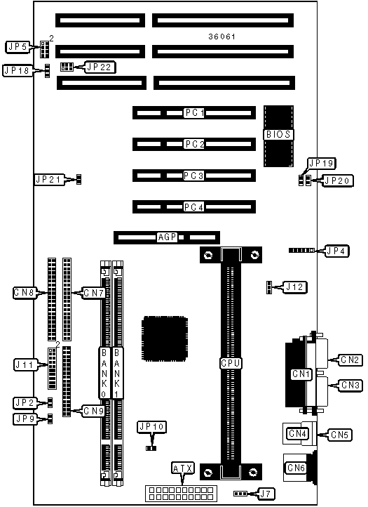
I/O Options |
32-bit PCI slots (4), floppy drive interface, green PC connector, IDE interfaces (2), parallel port, PS/2 mouse port, serial ports (2), IR connector, USB connectors (2), ATX power connector, AGP slot, wake on LAN connector, SB-link connector |
|
CONNECTIONS | |||
|
Purpose |
Location |
Purpose |
Location |
|
AGP slot |
AGP |
Turbo LED |
J11/pins 3 & 5 |
|
ATX power connector |
ATX |
Green PC connector |
J11/pins 7 & 9 |
|
Parallel port |
CN1 |
Speaker |
J11/pins 14/16/18/20 |
|
Serial port 2 |
CN2 |
Reset switch |
J11/pins 17 & 19 |
|
Serial port 1 |
CN3 |
Wake on LAN connector |
J12 |
|
USB connector 1 |
CN4 |
IDE interface LED |
JP2 |
|
USB connector 2 |
CN5 |
IR connector |
JP4 |
|
PS/2 mouse port |
CN6 |
Soft off power supply |
JP9 |
|
Floppy drive interface |
CN7 |
Temperature sensor |
JP10 |
|
IDE interface 2 |
CN8 |
Chassis fan power |
JP18 |
|
IDE interface 1 |
CN9 |
Chassis intrusion |
JP20 |
|
Chassis fan power |
J7 |
SB-link connector |
JP22 |
|
Power LED & keylock |
J11/pins 2/4/6/8/10 |
32-bit PCI slots |
PC1 - PC4 |
|
USER CONFIGURABLE SETTINGS | |||
|
Function |
Label |
Position | |
|
Power state function enabled |
JP19 |
Closed | |
|
Power state function disabled |
JP19 |
Open | |
|
DIMM CONFIGURATION | ||
|
Size |
Bank 0 |
Bank 1 |
|
8MB |
(1) 1M x 64 |
None |
|
16MB |
(1) 2M x 64 |
None |
|
16MB |
(1) 1M x 64 |
(1) 1M x 64 |
|
24MB |
(1) 2M x 64 |
(1) 1M x 64 |
|
32MB |
(1) 4M x 64 |
None |
|
32MB |
(1) 2M x 64 |
(1) 2M x 64 |
|
40MB |
(1) 4M x 64 |
(1) 1M x 64 |
|
48MB |
(1) 4M x 64 |
(1) 2M x 64 |
|
64MB |
(1) 8M x 64 |
None |
|
64MB |
(1) 4M x 64 |
(1) 4M x 64 |
|
72MB |
(1) 8M x 64 |
(1) 1M x 64 |
|
80MB |
(1) 8M x 64 |
(1) 2M x 64 |
|
96MB |
(1) 8M x 64 |
(1) 4M x 64 |
|
128MB |
(1) 16M x 64 |
None |
|
128MB |
(1) 8M x 64 |
(1) 8M x 64 |
|
136MB |
(1) 16M x 64 |
(1) 1M x 64 |
|
144MB |
(1) 16M x 64 |
(1) 2M x 64 |
|
160MB |
(1) 16M x 64 |
(1) 4M x 64 |
|
192MB |
(1) 16M x 64 |
(1) 8M x 64 |
|
256MB |
(1) 16M x 64 |
(1) 16M x 64 |
|
Note: Board accepts EDO & SDRAM memory. | ||
|
CACHE CONFIGURATION |
|
Note: 256KB/512KB cache is located on the Pentium II CPU. 128KB cache is located on the Celeron 300A & 333 CPU. |
|
CPU SPEED SELECTION | ||||
|
CPU speed |
Clock speed |
Multiplier |
JP5 |
JP21 |
|
233MHz |
66MHz |
3.5x |
1 & 2, 7 & 8 |
Closed |
|
266MHz |
66MHz |
4x |
1 & 2, 3 & 4, 5 & 6 |
Closed |
|
300MHz |
66MHz |
4.5x |
1 & 2, 5 & 6 |
Closed |
|
333MHz |
66MHz |
5x |
1 & 2, 3 & 4 |
Closed |
|
366MHz |
66MHz |
5.5x |
1 & 2 |
Closed |
|
350MHz |
100MHz |
3.5x |
1 & 2, 7 & 8 |
Open |
|
400MHz |
100MHz |
4x |
1 & 2, 3 & 4, 5 & 6 |
Open |
|
450MHz |
100MHz |
4.5x |
1 & 2, 5 & 6 |
Open |
|
500MHz |
100MHz |
5x |
1 & 2, 3 & 4 |
Open |
|
550MHz |
100MHz |
5.5x |
1 & 2 |
Open |
|
Note: Pins designated should be in the closed position. | ||||