UNIDENTIFIED
WIZ-286 KW-211
|
Processor |
80286 |
|
Processor Speed |
12MHz |
|
Chip Set |
SMD |
|
Max. Onboard DRAM |
4MB |
|
Cache |
None |
|
BIOS |
AMI |
|
Dimensions |
330mm x 218mm |
|
I/O Options |
Serial ports (2) |
|
NPU Options |
80287 |
|
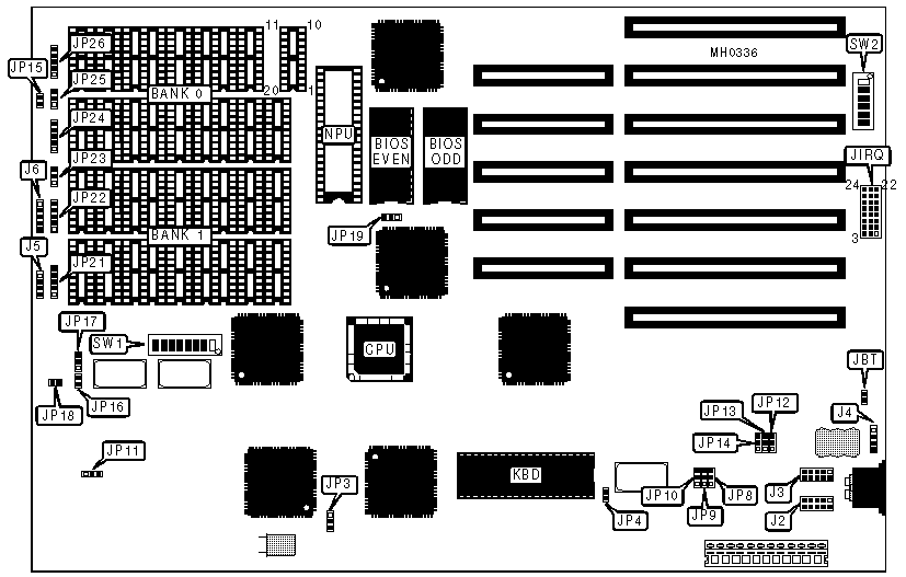
CONNECTIONS | |||
|
Purpose |
Location |
Purpose |
Location |
|
Serial port 2 |
J2 |
Power LED & keylock |
J6 |
|
Serial port 1 |
J3 |
Reset switch |
JP15 |
|
External battery |
J4 |
Turbo LED |
JP16 |
|
Speaker |
J5 |
Turbo switch |
JP18 |
|
USER CONFIGURABLE SETTINGS | |||
|
Function |
Jumper/Switch |
Position | |
| » |
CMOS memory normal operation |
JBT |
Closed |
|
CMOS memory clear |
JBT |
Open | |
| » |
Factory configured - do not alter |
JP3 |
N/A |
| » |
Monitor type select color |
JP4 |
Closed |
|
Monitor type select monochrome |
JP4 |
Open | |
| » |
Factory configured - do not alter |
JP11 |
pins 2 & 3 closed |
|
BIOS type select EPROM |
JP11 |
pins 1 & 2 closed | |
| » |
Factory configured - do not alter |
JP17 |
pins 2 & 3 closed |
|
CPU speed select switchable at turbo switch |
JP17 |
pins 1 & 2 closed | |
| » |
Factory configured - do not alter |
JP19 |
pins 2 & 3 closed |
|
BIOS ROM select 27256 |
JP19 |
pins 1 & 2 closed | |
| » |
Factory configured - do not alter |
SW1/1 |
N/A |
| » |
Factory configured - do not alter |
SW1/5 |
N/A |
| » |
Bus speed select ATCLK/1 |
SW1/6 |
Off |
|
Bus speed select ATCLK/2 |
SW1/6 |
On | |
| » |
DMA speed select CPU/1 |
SW1/7 |
Off |
|
DMA speed select CPU/2 |
SW1/7 |
On | |
| » |
Factory configured - do not alter |
SW1/8 |
N/A |
|
DRAM CONFIGURATION | ||
|
Size |
Bank 0 |
Bank 1 |
|
512KB |
(18) 41256 |
NONE |
|
640KB |
(18) 41256 |
(18) 4164 |
|
1MB |
(18) 41256 |
(18) 41256 |
|
2MB |
(18) 411000 |
NONE |
|
4MB |
(18) 411000 |
(18) 411000 |
|
Note:41256 and 4164 chips are placed in DIP socket pins 1 through 8 and 13 through 20. 411000 chips are placed in DIP socket pins 2 through 19. See upper right corner DIP socket on diagram for orientation. | ||
|
DRAM SWITCH CONFIGURATION | |||
|
Size |
SW1/2 |
SW1/3 |
SW1/4 |
|
512KB |
N/A |
Off |
Off |
|
640KB |
Off |
On |
Off |
|
1MB |
On |
On |
Off |
|
2MB |
N/A |
Off |
On |
|
4MB |
N/A |
On |
On |
|
DRAM JUMPER CONFIGURATION | ||||||
|
Size |
JP21 |
JP22 |
JP23 |
JP24 |
JP25 |
JP26 |
|
512KB |
2 & 3, 4 & 5 |
2 & 3, 4 & 5 |
2 & 3 |
2 & 3, 4 & 5 |
2 & 3 |
2 & 3, 4 & 5 |
|
640KB |
2 & 3, 4 & 5 |
2 & 3, 4 & 5 |
2 & 3 |
2 & 3, 4 & 5 |
2 & 3 |
2 & 3, 4 & 5 |
|
1MB |
2 & 3, 4 & 5 |
2 & 3, 4 & 5 |
2 & 3 |
2 & 3, 4 & 5 |
2 & 3 |
2 & 3, 4 & 5 |
|
2MB |
1 & 2, 3 & 4 |
1 & 2, 3 & 4 |
1 & 2 |
1 & 2, 3 & 4 |
1 & 2 |
1 & 2, 3 & 4 |
|
4MB |
1 & 2, 3 & 4 |
1 & 2, 3 & 4 |
1 & 2 |
1 & 2, 3 & 4 |
1 & 2 |
1 & 2, 3 & 4 |
|
Note:Pins designated should be in the closed position. | ||||||
|
IRQ CONFIGURATION | ||
|
Line |
IRQ for Serial port 1 |
IRQ for Serial port 2 |
|
IRQ3 |
pins 2 & 3 closed |
pins 1 & 2 closed |
|
IRQ4 |
pins 5 & 6 closed |
pins 4 & 5 closed |
|
IRQ5 |
pins 8 & 9 closed |
pins 7 & 8 closed |
|
IRQ9 |
pins 11 & 12 closed |
pins 10 & 11 closed |
|
IRQ10 |
pins 14 & 15 closed |
pins 13 & 14 closed |
|
IRQ11 |
pins 17 & 18 closed |
pins 16 & 17 closed |
|
IRQ12 |
pins 20 & 21 closed |
pins 19 & 20 closed |
|
IRQ15 |
pins 23 & 24 closed |
pins 22 & 23 closed |
|
SERIAL PORT 1 CONFIGURATION | |||
|
Setting |
JP8 |
JP9 |
JP10 |
|
Ready signal normal |
pins 1 & 2 closed |
pins 1 & 2 closed |
pins 1 & 2 closed |
|
Ready signal forced active |
pins 2 & 3 closed |
pins 2 & 3 closed |
pins 2 & 3 closed |
|
SERIAL PORT 2 CONFIGURATION | |||
|
Setting |
JP8 |
JP9 |
JP10 |
|
Ready signal normal |
pins 1 & 2 closed |
pins 1 & 2 closed |
pins 2 & 3 closed |
|
Ready signal forced active |
pins 2 & 3 closed |
pins 2 & 3 closed |
pins 2 & 3 closed |
|
SERIAL PORT 1 CONFIGURATION | |||
|
I/O Address |
SW2/1 |
SW2/2 |
SW2/3 |
|
COM1 |
On |
On |
Off |
|
COM2 |
On |
Off |
On |
|
COM3 |
On |
Off |
Off |
|
COM4 |
Off |
On |
On |
|
COM5 |
Off |
On |
Off |
|
COM6 |
Off |
Off |
On |
|
COM7 |
Off |
Off |
Off |
|
SERIAL PORT 2 CONFIGURATION | |||
|
I/O Address |
SW2/4 |
SW2/5 |
SW2/6 |
|
COM2 |
On |
On |
Off |
|
COM3 |
On |
Off |
On |
|
COM4 |
On |
Off |
Off |
|
COM5 |
Off |
On |
On |
|
COM6 |
Off |
On |
Off |
|
COM7 |
Off |
Off |
On |
|
COM8 |
Off |
Off |
Off |