WYSE TECHNOLOGY, INC.
WYSE PC 386 MODEL 3116SX
|
Processor |
80386SX |
|
Processor Speed |
16MHz |
|
Chip Set |
WYSE |
|
Max. Onboard DRAM |
12MB |
|
Cache |
None |
|
BIOS |
WYSE |
|
Dimensions |
334mm x 122mm |
|
I/O Options |
Serial ports (2) |
|
NPU Options |
80387SX |
|
CONNECTIONS | |||
|
Purpose |
Location |
Purpose |
Location |
|
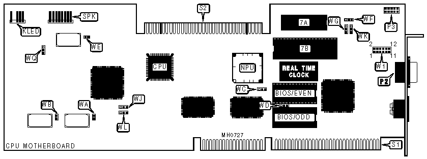
Power LED/Keylock |
KLED |
Speaker |
SPK |
|
Card edge connector |
S1 |
Serial port 2 |
P2 |
|
Top-Plane edge connector |
S2 |
Serial port 1 |
P3 |
|
USER CONFIGURABLE SETTINGS | |||
|
Function |
Jumper |
Position | |
| » |
Factory configured - do not alter |
WA |
Closed |
| » |
Factory configured - do not alter |
WB |
Closed |
| » |
Factory configured - do not alter |
WE |
Closed |
| » |
Factory test disabled |
WF |
pins 1 & 2 closed |
|
Factory test enabled |
WF |
pins 2 & 3 closed | |
| » |
Monitor type select color |
WG |
pins 1 & 2 closed |
|
Monitor type select monochrome |
WG |
pins 2 & 3 closed | |
| » |
NPU disabled |
WJ |
pins 2 & 3 closed |
|
NPU enabled |
WJ |
pins 1 & 2 closed | |
| » |
Keyboard controller chip at 7A select 6805 |
WK |
pins 2 & 3 closed |
|
Keyboard controller chip at 7A select 68705 |
WK |
pins 1 & 2 closed | |
| » |
ROM BIOS chips installed 2 |
WL |
pins 1 & 2 closed |
|
ROM BIOS chip installed 1 |
WL |
pins 2 & 3 closed | |
| » |
Factory configured - do not alter |
WQ |
pins 1 & 2 closed |
|
BIOS CONFIGURATION | ||
|
Size |
WC |
WD |
|
27128 |
pins 2 & 3 closed |
pins 2 & 3 closed |
|
27256 |
pins 1 & 2 closed |
pins 2 & 3 closed |
|
27512 |
pins 1 & 2 closed |
pins 1 & 2 closed |
|
KEYBOARD CONFIGURATION | |
|
Type |
W1 |
|
7B select 250646-XX |
Open |
|
7B select 250230-12/193002-12 7A must be empty |
1 & 2, 3 & 4, 5 & 6, 7 & 8, 9 & 10, 11 & 12 |
|
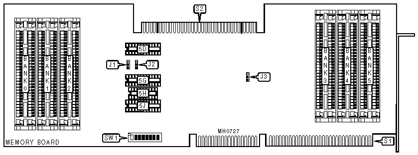
DRAM CONFIGURATION | ||||||
|
Size |
Bank 0 |
Bank 1 |
Bank 2 |
Bank 3 |
Bank 4 |
Bank 5 |
|
1MB 1 |
(2) 256K x 9 |
(2) 256K x 9 |
NONE |
NONE |
NONE |
NONE |
|
2MB 1 |
(2) 256K x 9 |
(2) 256K x 9 |
(2) 256K x 9 |
(2) 256K x 9 |
NONE |
NONE |
|
2MB 2 |
(2) 1M x 9 |
NONE |
NONE |
NONE |
NONE |
NONE |
|
4MB 1 |
(2) 256K x 9 |
(2) 256K x 9 |
(2) 256K x 9 |
(2) 256K x 9 |
(2) 1M x 9 |
NONE |
|
4MB 2 |
(2) 1M x 9 |
(2) 1M x 9 |
NONE |
NONE |
NONE |
NONE |
|
6MB 1 |
(2) 256K x 9 |
(2) 256K x 9 |
(2) 256K x 9 |
(2) 256K x 9 |
(2) 1M x 9 |
(2) 1M x 9 |
|
6MB 2 |
(2) 1M x 9 |
(2) 1M x 9 |
(2) 1M x 9 |
NONE |
NONE |
NONE |
|
8MB 2 |
(2) 1M x 9 |
(2) 1M x 9 |
(2) 1M x 9 |
(2) 1M x 9 |
NONE |
NONE |
|
10MB 2 |
(2) 1M x 9 |
(2) 1M x 9 |
(2) 1M x 9 |
(2) 1M x 9 |
(2) 1M x 9 |
NONE |
|
12MB 2 |
(2) 1M x 9 |
(2) 1M x 9 |
(2) 1M x 9 |
(2) 1M x 9 |
(2) 1M x 9 |
(2) 1M x 9 |
|
Note 1 :Using PAL configuration oneNote 2 :Using PAL configuration two | ||||||
|
DRAM JUMPER CONFIGURATION | |||
|
PAL configuration 1 | |||
|
Size |
Jumper J1 |
Jumper J2 |
Jumper J3 |
|
1MB |
pins 1 & 2 closed |
pins 1 & 2 closed |
pins 2 & 3 closed |
|
2MB |
pins 1 & 2 closed |
pins 1 & 2 closed |
pins 2 & 3 closed |
|
4MB |
pins 1 & 2 closed |
pins 1 & 2 closed |
pins 1 & 2 closed |
|
6MB |
pins 1 & 2 closed |
pins 1 & 2 closed |
pins 2 & 3 closed |
|
PAL configuration 2 | |||
|
2MB |
pins 1 & 2 closed |
pins 1 & 2 closed |
pins 1 & 2 closed |
|
4MB |
pins 1 & 2 closed |
pins 2 & 3 closed |
pins 1 & 2 closed |
|
6MB |
pins 1 & 2 closed |
pins 2 & 3 closed |
pins 1 & 2 closed |
|
8MB |
pins 2 & 3 closed |
pins 2 & 3 closed |
pins 1 & 2 closed |
|
10MB |
pins 2 & 3 closed |
pins 2 & 3 closed |
pins 1 & 2 closed |
|
12MB |
pins 2 & 3 closed |
pins 2 & 3 closed |
pins 2 & 3 closed |
|
DRAM SWITCH CONFIGURATION | |||||
|
PAL configuration 2 | |||||
|
Size |
SW1/1 |
SW1/2 |
SW1/3 |
SW1/4 |
SW1/8 |
|
1MB |
Off |
Off |
On |
Off |
On |
|
2MB |
Off |
On |
Off |
Off |
On |
|
4MB |
On |
Off |
Off |
Off |
On |
|
6MB |
Off |
Off |
Off |
Off |
On |
|
PAL configuration 2 | |||||
|
2MB |
On |
Off |
On |
On |
Off |
|
4MB |
Off |
Off |
On |
On |
Off |
|
6MB |
On |
On |
Off |
On |
Off |
|
8MB |
Off |
On |
Off |
On |
Off |
|
10MB |
On |
Off |
Off |
On |
Off |
|
12MB |
Off |
Off |
Off |
On |
Off |
|
PAL CHIP CONFIGURATION | ||||
|
Size |
Location 5D |
Location 5G |
Location 5H |
Location 5J |
|
Configuration 1 |
PAL chip 250-670-01 |
PAL chip 250-671-01 |
PAL chip 250-672-01 |
PAL chip 250-673-01 |
|
Configuration 2 |
PAL chip 250-680-01 |
PAL chip 250-681-01 |
PAL chip 250-682-01 |
PAL chip 250-683-01 |
|
Note:Order package WY-925 from WYSE to change PAL chip configurations. | ||||
|
MEMORY SPLIT CONFIGURATION | |||
|
Memory Split |
SW1/5 |
SW1/6 |
SW1/7 |
|
256KB/768KB |
Off |
On |
On |
|
512KB/512KB |
On |
Off |
On |
|
640KB/384KB |
Off |
Off |
On |
|
Disabled |
Off |
Off |
Off |