WYSE TECHNOLOGY, INC.
WYSE SERIES 3000I (MODEL 350)
|
Processor |
80486SX/80486DX/80486DX2 |
|
Processor Speed |
16/20/25/33/50(internal)/66(internal)MHz |
|
Chip Set |
Wyse |
|
Max. Onboard DRAM |
64MB |
|
Cache |
64/256KB |
|
BIOS |
Wyse |
|
Dimensions |
330mm x 218mm |
|
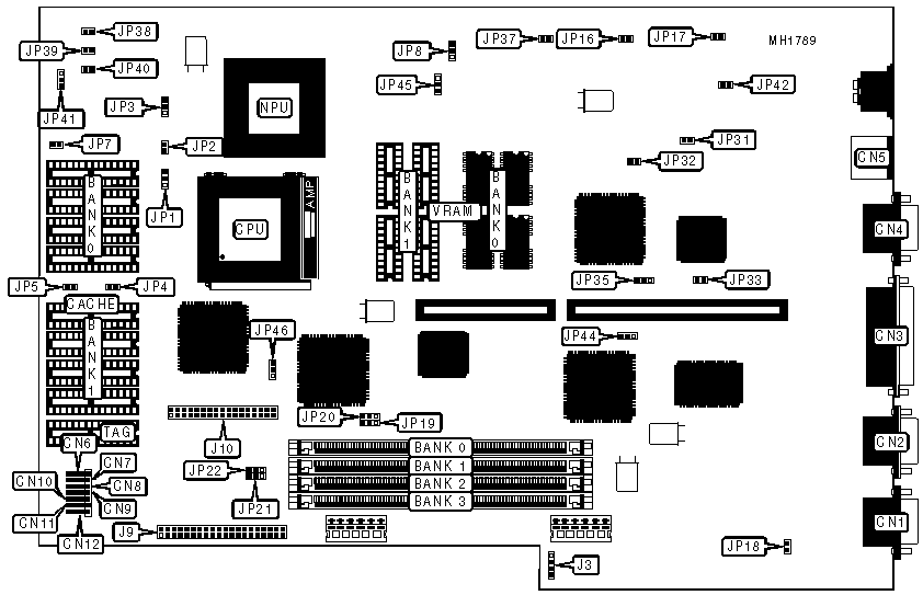
I/O Options |
Bus mouse port, floppy drive interface, IDE interface, parallel port, serial ports (2), VGA port |
|
NPU Options |
4167 |
|
CONNECTIONS | |||
|
Purpose |
Location |
Purpose |
Location |
|
Serial port 2 |
CN1 |
Reset switch |
CN9 |
|
Serial port 1 |
CN2 |
Keylock |
CN10 |
|
Parallel port |
CN3 |
Key connector |
CN11 |
|
VGA port |
CN4 |
Hard drive LED |
CN12 |
|
Bus mouse port |
CN5 |
External battery |
J3 |
|
Speaker |
CN6 |
IDE interface LED |
J9 |
|
Power LED |
CN7 |
Floppy drive interface |
J10 |
|
Turbo LED |
CN8 | ||
|
USER CONFIGURABLE SETTINGS | |||
|
Function |
Jumper |
Position | |
|
» |
Monitor type select color |
JP16 |
Closed |
|
Monitor type select monochrome |
JP16 |
Open | |
|
» |
Factory configured - do not alter |
JP17 |
Open |
|
» |
IDE interface enabled |
JP18 |
Open |
|
IDE interface disabled |
JP18 |
Closed | |
|
» |
Factory configured - do not alter |
JP19 |
Open |
|
» |
Factory configured - do not alter |
JP20 |
Open |
|
» |
Factory configured - do not alter |
JP21 |
Open |
|
» |
Factory configured - do not alter |
JP22 |
Open |
|
» |
Video interrupt IRQ2 disabled |
JP33 |
Open |
|
Video interrupt IRQ2 enabled |
JP33 |
Closed | |
|
» |
Video chipset ET4000 VGA (Rev. G) |
JP37 |
Closed |
|
Video chipset ET4000 VGA (Rev. F) |
JP37 |
Open | |
|
» |
Clock generator |
JP41 |
pins 1 & 2 closed |
|
Clock generator Oscillator (backup) |
JP41 |
pins 2 & 3 closed | |
|
» |
WY-790 select enabled |
JP42 |
Closed |
|
WY-790 select disabled |
JP42 |
Open | |
|
» |
External board diskette controller IRQ7 |
JP44 |
pins 1 & 2 closed |
|
External board diskette controller IRQ5 |
JP44 |
pins 2 & 3 closed | |
|
» |
Linear address enabled |
JP46 |
pins 1 & 2 closed |
|
Linear address disabled |
JP46 |
pins 2 & 3 closed | |
|
DRAM CONFIGURATION | ||||
|
Size |
Bank 0 |
Bank 1 |
Bank 2 |
Bank 3 |
|
1MB |
(1) 256K x 36 |
NONE |
NONE |
NONE |
|
2MB |
(1) 256K x 36 |
(1) 256K x 36 |
NONE |
NONE |
|
4MB |
(1) 1M x 36 |
NONE |
NONE |
NONE |
|
5MB |
(1) 256K x 36 |
(1) 1M x 36 |
NONE |
NONE |
|
6MB |
(1) 256K x 36 |
(1) 256K x 36 |
(1) 1M x 36 |
NONE |
|
8MB |
(1) 1M x 36 |
(1) 1M x 36 |
NONE |
NONE |
|
9MB |
(1) 256K x 36 |
(1) 1M x 36 |
(1) 1M x 36 |
NONE |
|
10MB |
(1) 256K x 36 |
(1) 256K x 36 |
(1) 1M x 36 |
(1) 1M x 36 |
|
12MB |
(1) 1M x 36 |
(1) 1M x 36 |
(1) 1M x 36 |
NONE |
|
13MB |
(1) 256K x 36 |
(1) 1M x 36 |
(1) 1M x 36 |
(1) 1M x 36 |
|
16MB |
(1) 4M x 36 |
NONE |
NONE |
NONE |
|
16MB |
(1) 1M x 36 |
(1) 1M x 36 |
(1) 1M x 36 |
(1) 1M x 36 |
|
20MB |
(1) 4M x 36 |
(1) 1M x 36 |
(1) 1M x 36 |
NONE |
|
20MB |
(1) 1M x 36 |
(1) 4M x 36 |
NONE |
NONE |
|
24MB |
(1) 1M x 36 |
(1) 1M x 36 |
(1) 4M x 36 |
NONE |
|
24MB |
(1) 1M x 36 |
(1) 4M x 36 |
(1) 1M x 36 |
NONE |
|
24MB |
(1) 4M x 36 |
(1) 1M x 36 |
(1) 1M x 36 |
NONE |
|
32MB |
(1) 4M x 36 |
(1) 4M x 36 |
NONE |
NONE |
|
36MB |
(1) 4M x 36 |
(1) 1M x 36 |
(1) 4M x 36 |
NONE |
|
36MB |
(1) 1M x 36 |
(1) 4M x 36 |
(1) 4M x 36 |
NONE |
|
36MB |
(1) 4M x 36 |
(1) 4M x 36 |
(1) 1M x 36 |
NONE |
|
DRAM CONFIGURATION (CONT.) | ||||
|
Size |
Bank 0 |
Bank 1 |
Bank 2 |
Bank 3 |
|
40MB |
(1) 1M x 36 |
(1) 1M x 36 |
(1) 4M x 36 |
(1) 4M x 36 |
|
40MB |
(1) 1M x 36 |
(1) 4M x 36 |
(1) 4M x 36 |
(1) 1M x 36 |
|
40MB |
(1) 4M x 36 |
(1) 4M x 36 |
(1) 1M x 36 |
(1) 1M x 36 |
|
48MB |
(1) 4M x 36 |
(1) 4M x 36 |
(1) 4M x 36 |
NONE |
|
52MB |
(1) 1M x 36 |
(1) 4M x 36 |
(1) 4M x 36 |
(1) 4M x 36 |
|
52MB |
(1) 4M x 36 |
(1) 1M x 36 |
(1) 4M x 36 |
(1) 4M x 36 |
|
52MB |
(1) 4M x 36 |
(1) 4M x 36 |
(1) 4M x 36 |
(1) 1M x 36 |
|
64MB |
(1) 4M x 36 |
(1) 4M x 36 |
(1) 4M x 36 |
(1) 4M x 36 |
|
CACHE CONFIGURATION | |||
|
Size |
Bank 0 |
Bank 1 |
TAG |
|
0KB |
NONE |
NONE |
NONE |
|
64KB |
(4) 8K x 8 |
(4) 8K x 8 |
(1) 8K x 8 |
|
256KB |
(4) 32K x 8 |
(4) 32K x 8 |
(1) 32K x 8 |
|
Note:The exact locations of Bank 0 and Bank 1 are unknown. | |||
|
CACHE JUMPER CONFIGURATION | |||
|
Size |
JP4 |
JP5 |
JP7 |
|
0KB |
Open |
Open |
Open |
|
64KB |
Open |
Open |
Open |
|
256KB |
Closed |
Closed |
Closed |
|
CPU TYPE CONFIGURATION | |||
|
Type |
JP1 |
JP2 |
JP3 |
|
80486SX |
Open |
Open |
pins 2 & 3 closed |
|
80486DX |
pins 2 & 3 closed |
pins 1 & 2 closed |
pins 1 & 2 closed |
|
80486DX2 |
pins 2 & 3 closed |
pins 1 & 2 closed |
pins 1 & 2 closed |
|
CPU SPEED CONFIGURATION | |||
|
Speed |
JP38 |
JP39 |
JP40 |
|
16MHz |
pins 1 & 2 closed |
Open |
pins 1 & 2 closed |
|
20MHz |
pins 1 & 2 closed |
Open |
Open |
|
25MHz |
Open |
pins 1 & 2 closed |
pins 1 & 2 closed |
|
33MHz |
Open |
pins 1 & 2 closed |
Open |
|
50iMHz |
Open |
pins 1 & 2 closed |
pins 1 & 2 closed |
|
66iMHz |
Open |
pins 1 & 2 closed |
Open |
|
VGA WAIT STATE | |||
|
Wait states |
JP31 |
JP32 | |
| » |
1 wait state |
Closed |
Closed |
|
0 wait states |
pins 1 & 2 closed |
Open | |
|
VGA SELECT | |||
|
Setting |
JP8 |
JP35 |
JP45 |
|
Enabled |
pins 1 & 2 closed |
pins 1 & 2 closed |
pins 1 & 2 closed |
|
Disabled |
pins 2 & 3 closed |
pins 2 & 3 closed |
pins 2 & 3 closed |
|
VRAM MEMORY CONFIGURATION | ||
|
Size |
Bank 0 |
Bank 1 |
|
512KB |
(4) 44256 |
NONE |
|
1MB |
(4) 44256 |
(4) 44256 |