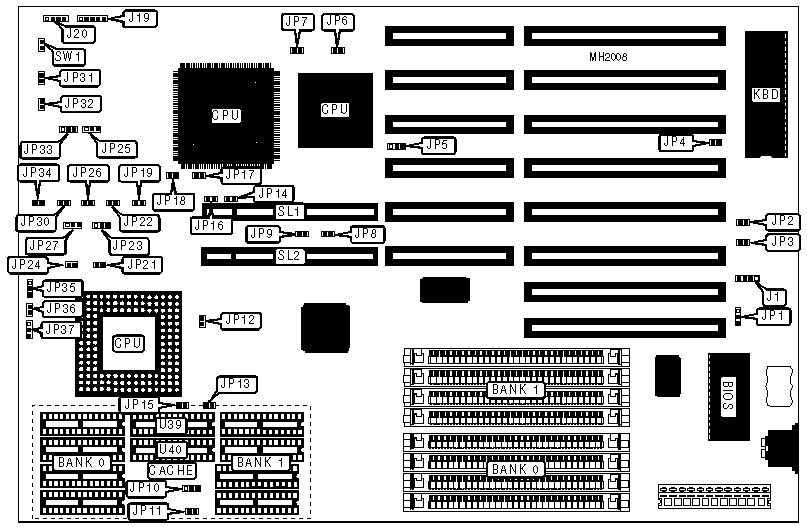
UNIDENTIFIED
VESA X86VLWB
|
Processor |
80386DX/80486SX/80486DX/80486DX2 |
|
Processor Speed |
25/33/40/50(internal)/66(internal)MHz |
|
Chip Set |
Intel |
|
Max. Onboard DRAM |
32MB |
|
Cache |
64/128/256KB |
|
BIOS |
AMI |
|
Dimensions |
330mm x 218mm |
|
I/O Options |
32-bit VESA local bus slots (2) |
|
NPU Options |
80387DX |
|
CONNECTIONS | |||
|
Purpose |
Location |
Purpose |
Location |
|
External battery |
J1 |
Turbo LED |
JP32 |
|
Power LED & keylock |
J19 |
32-bit VESA Local bus slots |
SL1, SL2 |
|
Speaker |
J20 |
Reset switch |
SW1 |
|
Turbo switch |
JP31 | ||
|
USER CONFIGURABLE SETTINGS | |||
|
Function |
Jumper |
Position | |
|
» |
CMOS normal operation |
JP1 |
pins 2 & 3 closed |
|
CMOS memory clear |
JP1 |
pins 1 & 2 closed | |
|
Bus speed select - Clock/5 |
JP3 |
Closed | |
|
Bus speed select - Clock/4 |
JP3 |
Open | |
|
» |
Monitor type select monochrome |
JP4 |
Closed |
|
Monitor type select color |
JP4 |
Open | |
|
» |
Factory configured - do not alter |
JP16 |
Open |
|
Enable 486SX PQFP |
JP17 |
Open | |
|
Disable 486SX PQFP |
JP17 |
Closed | |
|
Enable 386DX PQFP |
JP18 |
Open | |
|
Disable 386DX PQFP |
JP18 |
Closed | |
|
DRAM CONFIGURATION | ||
|
Size |
Bank 0 |
Bank 1 |
|
1MB |
(4) 256K x 9 |
NONE |
|
2MB |
(4) 256K x 9 |
(4) 256K x 9 |
|
4MB |
(4) 1M x 9 |
NONE |
|
5MB |
(4) 256K x 9 |
(4) 1M x 9 |
|
8MB |
(4) 1M x 9 |
(4) 1M x 9 |
|
16MB |
(4) 4M x 9 |
NONE |
|
20MB |
(4) 1M x 9 |
(4) 4M x 9 |
|
20MB |
(4) 4M x 9 |
(4) 1M x 9 |
|
32MB |
(4) 4M x 9 |
(4) 4M x 9 |
|
PROCESSOR TYPE CONFIGURATION | |||
|
Type |
JP2 |
JP6 |
JP7 |
|
Cyrix |
Closed |
Closed |
Closed |
|
Intel/AMD |
Open |
Open |
Open |
|
CPU TYPE CONFIGURATION | ||
|
Type |
JP5 |
JP12 |
|
80386 |
pins 2 & 3 closed |
Closed |
|
80486 |
pins 1 & 2 closed |
Open |
|
CPU CLOCK CONFIGURATION | |||
|
Type |
Speed |
JP25 |
JP33 |
|
80386DX |
25MHz |
pins 2 & 3 closed |
pins 1 & 2 closed |
|
80386DX |
33MHz |
pins 2 & 3 closed |
pins 1 & 2 closed |
|
80486SX |
25MHz |
pins 2 & 3 closed |
pins 2 & 3 closed |
|
80486SX |
33MHz |
pins 2 & 3 closed |
pins 2 & 3 closed |
|
80486DX |
33MHz |
pins 2 & 3 closed |
pins 2 & 3 closed |
|
80486DX |
50MHz |
pins 1 & 2 closed |
pins 1 & 2 closed |
|
80486DX2 |
50iMHz |
pins 1 & 2 closed |
pins 1 & 2 closed |
|
80486DX2 |
66iMHz |
pins 2 & 3 closed |
pins 2 & 3 closed |
|
486 PROCESSOR CONFIGURATION | |||
|
Type |
JP35 |
JP36 |
JP37 |
|
80486SX |
pins 2 & 3 closed |
Open |
pins 2 & 3 closed |
|
80486DX |
pins 1 & 2 closed |
Closed |
pins 1 & 2 closed |
|
80486DX2 |
pins 1 & 2 closed |
Closed |
pins 1 & 2 closed |
|
CACHE CONFIGURATION | ||||
|
Size |
Bank 0 |
Bank 1 |
TAG (U39) |
TAG (U40) |
|
64KB |
(4) 8K x 8 |
(4) 8K x 8 |
(1) 8K x 8 |
NONE |
|
128KB |
(4) 32K x 8 |
NONE |
(1) 8K x 8 |
NONE |
|
256KB |
(4) 32K x 8 |
(4) 32K x 8 |
(1) 8K x 8 |
(1) 8K x 8 |
|
CACHE JUMPER CONFIGURATION | ||||
|
Size |
JP10 |
JP11 |
JP13 |
JP15 |
|
64KB |
pins 2 & 3 closed |
Open |
Open |
Open |
|
128KB |
pins 2 & 3 closed |
Closed |
Closed |
Open |
|
256KB |
pins 1 & 2 closed |
Closed |
Closed |
Closed |
|
VESA CPU TYPE CONFIGURATION | ||
|
CPU Type |
JP30 |
JP34 |
|
80386 |
pins 2 & 3 closed |
pins 1 & 2 closed |
|
80486 |
pins 1 & 2 closed |
pins 2 & 3 closed |
|
VESA WAIT STATE CONFIGURATION | |||
|
CPU speed |
Wait states |
JP22 |
JP26 |
|
< 33MHz |
0 wait states |
Open |
Open |
|
> 33MHz |
1 wait states |
Closed |
Closed |
|
MISCELLANEOUS TECHNICAL NOTES |
|
Note:The VESA bus can be disabled by removing two integrated chips (IC) off the system board. |
|
To disable the VESA bus, ICs located on U29 and U38 must be removed and the following |
|
jumpers must be installed: JP8, JP9, JP14, JP19, JP21, JP23, JP24, JP27. |
|
To enable the VESA bus, insert two ICs at U29 and U38. And all jumpers in above paragraph |
|
must be open. |
|
Some system boards may have a clock generating device which must be set to generate the |
|
proper clock speed for the CPU. Jumpers JP28 and JP29 are used to set the clock frequency |
|
the device should generate. In most systems, this device is replaced with an oscillator. |