UNIDENTIFIED
J-286P SYSTEM BOARD
|
Processor |
80286 (exact location unknown) |
|
Processor Speed |
12/16/20/24MHz |
|
Chip Set |
Suntac |
|
Max. Onboard DRAM |
5MB |
|
Cache |
None |
|
BIOS |
AMI |
|
Dimensions |
220mm x 220mm |
|
I/O Options |
Floppy drive interface (on some models), IDE interface (on some models) |
|
NPU Options |
80287 (exact location unknown) |
|
CONNECTIONS | |||
|
Purpose |
Location |
Purpose |
Location |
|
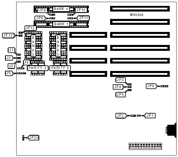
Reset switch |
J1 |
Speaker |
J4 |
|
Turbo switch |
J2 |
Power LED & keylock |
J5 |
|
Turbo LED |
J3 |
External battery |
JP9 |
|
USER CONFIGURABLE SETTINGS | |||
|
Function |
Jumper |
Position | |
|
» |
Factory configured - do not alter |
JP1 |
Open |
|
» |
Factory configured - do not alter |
JP2 |
Open |
|
» |
Floppy drive interface enabled (interface location unknown) |
JP5 |
Closed |
|
Floppy drive interface disabled |
JP5 |
Open | |
|
» |
Monitor type select monochrome |
JP12 |
Open |
|
Monitor type select color |
JP12 |
Closed | |
|
» |
Parity check enabled |
JP13 |
Closed |
|
Parity check disabled |
JP13 |
Open | |
|
DRAM CONFIGURATION | ||||||
|
Size |
Bank 0 |
Bank 1 |
Bank 2 |
Parity 2 |
Bank 3 |
Parity 3 |
|
1MB |
NONE |
NONE |
(4) 44256 |
(4) 41256 |
(4) 44256 |
(4) 41256 |
|
1MB |
(2) 256K x 9 |
(2) 256K x 9 |
NONE |
NONE |
NONE |
NONE |
|
2MB |
(2) 256K x 9 |
(2) 256K x 9 |
(4) 44256 |
(4) 41256 |
(4) 44256 |
(4) 41256 |
|
2MB |
(2) 1M x 9 |
NONE |
NONE |
NONE |
NONE |
NONE |
|
3MB |
(2) 1M x 9 |
NONE |
(4) 44256 |
(4) 41256 |
(4) 44256 |
(4) 41256 |
|
4MB |
(2) 1M x 9 |
(2) 1M x 9 |
NONE |
NONE |
NONE |
NONE |
|
5MB |
(2) 1M x 9 |
(2) 1M x 9 |
(4) 44256 |
(4) 41256 |
(4) 44256 |
(4) 41256 |
|
DRAM JUMPER CONFIGURATION | ||||
|
Size |
JP8 |
JP9 |
JP10 |
JP11 |
|
1MB |
pins 2 & 3 closed |
pins 2 & 3 closed |
pins 2 & 3 closed |
pins 2 & 3 closed |
|
1MB |
pins 1 & 2 closed |
pins 1 & 2 closed |
pins 1 & 2 closed |
pins 1 & 2 closed |
|
2MB |
pins 2 & 3 closed |
pins 2 & 3 closed |
pins 2 & 3 closed |
pins 2 & 3 closed |
|
2MB |
pins 1 & 2 closed |
pins 1 & 2 closed |
pins 1 & 2 closed |
pins 1 & 2 closed |
|
3MB |
pins 2 & 3 closed |
pins 2 & 3 closed |
pins 2 & 3 closed |
pins 2 & 3 closed |
|
4MB |
pins 1 & 2 closed |
pins 1 & 2 closed |
pins 1 & 2 closed |
pins 1 & 2 closed |
|
5MB |
pins 2 & 3 closed |
pins 2 & 3 closed |
pins 2 & 3 closed |
pins 2 & 3 closed |
|
IDE INTERFACE CONFIGURATION | ||
|
Setting |
JP3 |
JP4 |
|
Enabled |
Closed |
Open |
|
Disabled |
Open |
Closed |
|
Note: The location of the interface is unknown. Interface is an option and may not be present. | ||
|
CPU SPEED CONFIGURATION | ||
|
System speed |
Bus speed |
JP20 |
|
12MHz |
6MHz |
pins 1 & 2 closed |
|
16MHz |
8MHz |
pins 1 & 2 closed |
|
20MHz |
8MHz |
pins 2 & 3 closed |
|
24MHz |
8MHz |
pins 2 & 3 closed |