UNIDENTIFIED
286A
|
Processor |
80286 |
|
Processor Speed |
12/16MHz |
|
Chip Set |
C & T |
|
Max. Onboard DRAM |
5MB |
|
Cache |
None |
|
BIOS |
AMI |
|
Dimensions |
310mm x 218mm |
|
I/O Options |
Floppy drive interface, game port, IDE interface, parallel port, serial ports (2) |
|
NPU Options |
80287 |
|
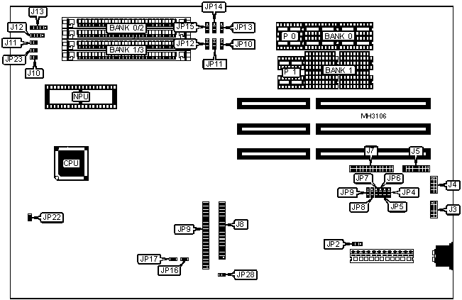
CONNECTIONS | |||
|
Purpose |
Location |
Purpose |
Location |
|
Serial port 2 |
J3 |
Reset switch |
J11 |
|
Serial port 1 |
J4 |
Speaker |
J12 |
|
Game port |
J5 |
Power LED & keylock |
J13 |
|
Parallel port |
J7 |
IDE interface |
JP9 |
|
Floppy drive interface |
J8 |
Turbo switch |
JP23 |
|
Turbo LED |
J10 |
IDE interface LED |
JP28 |
|
USER CONFIGURABLE SETTINGS | |||
|
Function |
Jumper |
Position | |
|
Monitor type select monochrome |
JP2 |
pins 1 & 2 closed | |
|
Monitor type select color |
JP2 |
pins 2 & 3 closed | |
|
Floppy drive interface enabled |
JP4 |
pins 1 & 2 closed | |
|
Floppy drive interface disabled |
JP4 |
pins 2 & 3 closed | |
|
CPU low speed CLK select 1/2 ATCLK |
JP22 |
Closed | |
|
CPU low speed CLK select 1/4 CLK2N |
JP22 |
Open | |
|
DRAM CONFIGURATION | ||||||
|
Size |
Bank 0 |
P 0 |
Bank 1 |
P 1 |
Bank 2 |
Bank 3 |
|
512KB |
(4) 44256 |
(2) 41256 |
NONE |
NONE |
NONE |
NONE |
|
640KB |
(4) 44256 |
(2) 41256 |
(4) 4464 |
(2) 4164 |
NONE |
NONE |
|
1MB |
(4) 44256 |
(2) 41256 |
(4) 44256 |
(2) 41256 |
NONE |
NONE |
|
2MB |
(4) 44256 |
(2) 41256 |
(4) 44256 |
(2) 41256 |
(2) 256K x 9 |
(2) 256K x 9 |
|
2MB |
NONE |
NONE |
NONE |
NONE |
(2) 1M x 9 |
NONE |
|
3MB |
(4) 44256 |
(2) 41256 |
(4) 44256 |
(2) 41256 |
(2) 1M x 9 |
NONE |
|
4MB |
NONE |
NONE |
NONE |
NONE |
(2) 1M x 9 |
(2) 1M x 9 |
|
5MB |
(4) 44256 |
(2) 41256 |
(4) 44256 |
(2) 41256 |
(2) 1M x 9 |
(2) 1M x 9 |
|
DRAM CONFIGURATION | ||||||
|
Setting |
JP10 |
JP11 |
JP12 |
JP13 |
JP14 |
JP15 |
|
SIMM set as Bank 0 & 1 |
1 & 2 |
1 & 2 |
1 & 2 |
1 & 2 |
1 & 2 |
1 & 2 |
|
SIMM set as Bank 2 & 3 |
2 & 3 |
2 & 3 |
2 & 3 |
2 & 3 |
2 & 3 |
2 & 3 |
|
Note: Pins designated should be in the closed position. | ||||||
|
IDE CONFIGURATION | ||
|
Setting |
JP16 |
JP17 |
|
Enabled |
Closed |
Closed |
|
Disabled |
Open |
Open |
|
PARALLEL PORT CONFIGURATION | ||
|
LPT |
JP8 |
JP9 |
|
LPT1 |
pins 1 & 2 closed |
pins 2 & 3 closed |
|
LPT2 |
pins 1 & 2 closed |
pins 1 & 2 closed |
|
LPT3 |
pins 2 & 3 closed |
pins 1 & 2 closed |
|
Disabled |
pins 2 & 3 closed |
pins 2 & 3 closed |
|
SERIAL PORT CONFIGURATION | ||||
|
Serial port 1 |
Serial port 2 |
JP5 |
JP6 |
JP7 |
|
COM1 |
COM2 |
pins 1 & 2 closed |
pins 1 & 2 closed |
pins 1 & 2 closed |
|
COM1 |
Disabled |
pins 1 & 2 closed |
pins 2 & 3 closed |
pins 1 & 2 closed |
|
COM2 |
COM1 |
pins 2 & 3 closed |
pins 1 & 2 closed |
pins 1 & 2 closed |
|
Disabled |
COM1 |
pins 2 & 3 closed |
pins 1 & 2 closed |
pins 2 & 3 closed |
|
Disabled |
COM2 |
pins 1 & 2 closed |
pins 1 & 2 closed |
pins 2 & 3 closed |
|
COM2 |
Disabled |
pins 2 & 3 closed |
pins 2 & 3 closed |
pins 1 & 2 closed |
|
Disabled |
Disabled |
pins 1 & 2 closed |
pins 2 & 3 closed |
pins 2 & 3 closed |