MOTOROLA, INC.
VANGUARD 300
|
Card Type |
Frame relay adapter, Ethernet router |
|
Processor |
Motorola 68360 |
|
Processor Speed |
Unidentified |
|
Chip Set |
Unidentified |
|
Maximum Onboard Memory |
8MB DRAM/2MB Flash RAM |
|
I/O Options |
Serial ports (3) |
|
Network Transfer Rate |
10Mbps |
|
DSU Transfer Rate |
56Kbps |
|
ISDN Transfer Rate |
64Kbps x 2 |
|
DSU Protocol |
DDS |
|
ISDN Protocol |
Unidentified |
|
Switch Type |
Unidentified |
|
Data Bus |
External |
|
Topology |
Linear Bus/Star |
|
Wiring Type |
Unshielded twisted pair AUI transceiver via DB-15 port |
|
Boot ROM |
Not available |
|
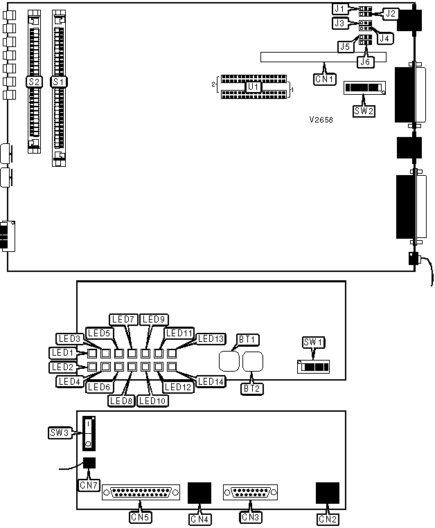
CONNECTIONS | |||
|
Function |
Label |
Function |
Label |
|
Reset button |
BT1 |
DECconnect MMJ connector or ISDN connector (port 4) |
CN4 |
|
Lamp test button |
BT2 |
V.24 serial port (port 3) |
CN5 |
|
Header for daughtercard |
CN1 |
V.11, V.24, V.35, or V.36 serial port (port 2) |
CN6 |
|
Unshielded twisted pair connector |
CN2 |
120VAC power |
CN7 |
|
AUI transceiver via DB-15 port |
CN3 |
Power switch |
SW3 |
|
Note:When LED4 is on, press the lamp test button to reset it. Port 1 is the daughterboard. | |||
|
USER CONFIGURABLE SETTINGS | |||
|
Setting |
Label |
Position | |
| » |
Port 2 pin 22 used for ring indicator |
SW1/1 |
Off |
|
Port 2 pin 22 used to enter test mode in DCE mode, ring indicator in DTE mode |
SW1/1 |
On | |
| » |
Port 2 pin 25 used for test mode indicator |
SW1/2 |
Off |
|
Port 2 pin 25 used for test mode indicator for DCE mode, busy out for DTE mode |
SW1/2 |
On | |
| » |
Port 3 pin 22 used for ring indicator |
SW1/3 |
Off |
|
Port 3 pin 22 used to enter test mode in DCE mode, ring indicator in DTE mode |
SW1/3 |
On | |
| » |
Port 3 is normal serial port |
SW1/4 |
Off |
|
Port 3 is the PAD port (forces serial configuration to 9600bps, no parity, 8 data bits, 1 stop bit) |
SW1/4 |
On | |
| » |
Factory configured - do not alter |
SW1/5 |
Off |
| » |
Normal operation |
SW1/6 |
Off |
|
Reset entire configuration to factory defaults |
SW1/6 |
On | |
|
Note:To use SW1/6, power up the adapter, turn SW1/6 on, press the reset button, and turn SW1/9 back off again. | |||
|
CABLE TYPE | |||
|
Setting |
J1 |
J2 |
J3 |
|
Unshielded twisted pair |
Pins 1 & 2 closed |
Pins 1 & 2 closed |
Pins 1 & 2 closed |
|
AUI transceiver via DB-15 port |
Pins 2 & 3 closed |
Pins 2 & 3 closed |
Pins 2 & 3 closed |
|
CABLE TYPE (CON’T) | |||
|
Setting |
J4 |
J5 |
J6 |
|
Unshielded twisted pair |
Pins 1 & 2 closed |
Pins 1 & 2 closed |
Pins 1 & 2 closed |
|
AUI transceiver via DB-15 port |
Pins 2 & 3 closed |
Pins 2 & 3 closed |
Pins 2 & 3 closed |
|
DRAM | ||
|
Setting |
On Board |
S1 |
|
4MB |
4MB |
None |
|
8MB |
4MB |
(1) 4MB x 9 |
|
PORT 2 TYPE | ||||||
|
Setting |
SW2/1 |
SW2/2 |
SW2/3 |
SW2/4 |
SW2/5 |
SW2/6 |
|
V.11 DTE |
Off |
Off |
Off |
Off |
Off |
On |
|
V.11 DCE |
Off |
Off |
Off |
Off |
Off |
On |
|
V.24 DTE |
On |
On |
On |
On |
On |
Off |
|
V.24 DCE |
On |
On |
On |
On |
On |
Off |
|
V.35 DTE |
Off |
Off |
Off |
Off |
Off |
On |
|
V.35 DCE |
Off |
Off |
Off |
Off |
Off |
On |
|
V.36 DTE |
Off |
Off |
Off |
Off |
Off |
On |
|
V.36 DCE |
Off |
Off |
Off |
Off |
Off |
On |
|
DSU |
Off |
Off |
Off |
Off |
Off |
On |
|
PORT 2 TYPE (CON’T) | |||
|
Setting |
SW2/7 |
SW2/8 |
U1 |
|
V.11 DTE |
On |
On |
V.11 module in position 1 |
|
V.11 DCE |
On |
On |
V.11 module in position 2 |
|
V.24 DTE |
Off |
Off |
V.24 module in position 1 |
|
V.24 DCE |
Off |
Off |
V.24 module in position 2 |
|
V.35 DTE |
On |
On |
V.35 module in position 1 |
|
V.35 DCE |
On |
On |
V.35 module in position 2 |
|
V.36 DTE |
On |
On |
V.36 module in position 1 |
|
V.36 DCE |
On |
On |
V.36 module in position 2 |
|
DSU |
On |
On |
DSU module in position 1 |
|
DIAGNOSTIC LED(S) (RESET AND POWER-UP) | ||
|
LED1 |
LED3 |
Condition |
|
Blinking |
Off |
Adapter is loading software into DRAM from flash RAM |
|
Off |
Blinking |
Adapter is performing self-test |
|
Off |
Off |
Adapter is initializing configuration |
|
On |
Off |
Adapter is ready |
|
Off |
On |
Self-test failed |
|
Note:On reset or power-up, the LEDs should go through, in order, the first four actions shown above. If the adapter proceeds immediately to the fourth action, the code in the firmware is invalid. | ||
|
DIAGNOSTIC LED(S) | |||
|
LED |
Color |
Status |
Condition |
|
LED1 |
Green |
On |
Software is running |
|
LED1 |
Green |
Off |
Software not running |
|
LED1 |
Green |
Blinking |
Software is downloading or card is booting |
|
LED2 |
Green |
On |
Power is on |
|
LED2 |
Green |
Off |
Power is off |
|
LED3 |
Red |
On |
Test failed |
|
LED3 |
Red |
Off |
No test in progress or test passed |
|
LED3 |
Red |
Blinking |
Test in progress |
|
LED4 |
Red |
On |
Processor did not reset timer in set time |
|
LED4 |
Red |
Off |
Normal operation |
|
LED5 |
Yellow |
On |
Card is transmitting MARK signal to port 1 |
|
LED5 |
Yellow |
Off |
Card is transmitting SPACE signal to port 1 |
|
LED6 |
Yellow |
On |
Card is receiving MARK signal from port 1 |
|
LED6 |
Yellow |
Off |
Card is receiving SPACE signal from port 1 |
|
LED7 |
Yellow |
On |
Card is transmitting MARK signal to port 2 |
|
LED7 |
Yellow |
Off |
Card is transmitting SPACE signal to port 2 |
|
LED8 |
Yellow |
On |
Card is receiving MARK signal from port 2 |
|
LED8 |
Yellow |
Off |
Card is receiving SPACE signal from port 2 |
|
LED9 |
Yellow |
On |
Card is transmitting MARK signal to port 3 |
|
LED9 |
Yellow |
Off |
Card is transmitting SPACE signal to port 3 |
|
LED10 |
Yellow |
On |
Card is receiving MARK signal from port 3 |
|
LED10 |
Yellow |
Off |
Card is receiving SPACE signal from port 3 |
|
LED11 |
Yellow |
On |
Card is transmitting MARK signal to port 4 |
|
LED11 |
Yellow |
Off |
Card is transmitting SPACE signal to port 4 |
|
LED12 |
Yellow |
On |
Card is receiving MARK signal from port 4 |
|
LED12 |
Yellow |
Off |
Card is receiving SPACE signal from port 4 |
|
LED13 |
Yellow |
On |
Card is transmitting MARK signal to network |
|
LED13 |
Yellow |
Off |
Card is transmitting SPACE signal to network |
|
LED14 |
Yellow |
On |
Card is receiving MARK signal from network |
|
LED14 |
Yellow |
Off |
Card is receiving SPACE signal from network |
|
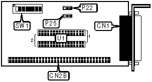
Card Type |
Serial |
|
I/O Options |
Serial port |
|
CONNECTIONS | |||
|
Function |
Label |
Function |
Label |
|
V.11 V.24, V.35, V.36, or DSU port |
CN1 |
Header to main board (on both front and back of card) |
CN2B |
|
USER CONFIGURABLE SETTINGS | |||
|
Setting |
Label |
Position | |
| » |
Pin 22 used for ring indicator |
P22 |
Pins 2 & 3 closed |
|
Pin 22 used to enter test mode in DCE mode, ring indicator in DTE mode |
P22 |
Pins 1 & 2 closed | |
| » |
Pin 25 used for test mode indicator |
P25 |
Pins 1 & 2 closed |
|
Pin 25 used for test mode indicator for DCE mode, busy out for DTE mode |
P25 |
Pins 2 & 3 closed | |
|
SERIAL PORT TYPE | ||||||
|
Setting |
SW1/1 |
SW1/2 |
SW1/3 |
SW1/4 |
SW1/5 |
SW1/6 |
|
V.11 DTE |
Off |
Off |
Off |
Off |
Off |
On |
|
V.11 DCE |
Off |
Off |
Off |
Off |
Off |
On |
|
V.24 DTE |
On |
On |
On |
On |
On |
Off |
|
V.24 DCE |
On |
On |
On |
On |
On |
Off |
|
V.35 DTE |
Off |
Off |
Off |
Off |
Off |
On |
|
V.35 DCE |
Off |
Off |
Off |
Off |
Off |
On |
|
V.36 DTE |
Off |
Off |
Off |
Off |
Off |
On |
|
V.36 DCE |
Off |
Off |
Off |
Off |
Off |
On |
|
DSU |
Off |
Off |
Off |
Off |
Off |
On |
|
SERIAL PORT TYPE (CON’T) | |||
|
Setting |
SW1/7 |
SW1/8 |
U1 |
|
V.11 DTE |
On |
On |
V.11 module in position 1 |
|
V.11 DCE |
On |
On |
V.11 module in position 2 |
|
V.24 DTE |
Off |
Off |
V.24 module in position 1 |
|
V.24 DCE |
Off |
Off |
V.24 module in position 2 |
|
V.35 DTE |
On |
On |
V.35 module in position 1 |
|
V.35 DCE |
On |
On |
V.35 module in position 2 |
|
V.36 DTE |
On |
On |
V.36 module in position 1 |
|
V.36 DCE |
On |
On |
V.36 module in position 2 |
|
DSU |
On |
On |
DSU module in position 1 |
|
Card Type |
ISDN TA |
|
ISDN Transfer Rate |
64Kbps x 2 |
|
ISDN Protocol |
Unidentified |
|
Switch Type |
Unidentified |

|
CONNECTIONS | |||
|
Function |
Label |
Function |
Label |
|
Line in/out |
CN1 |
Line in/out |
CN3 |
|
Header to main board (on both front and back of card) |
CN2B | ||
|
Note:Two connectors are provided so the user can daisy-chain devices on the S/T bus. | |||
|
USER CONFIGURABLE SETTINGS | |||
|
Setting |
Label |
Position | |
| » |
S/T bus not terminated |
SW1 |
Off |
|
S/T bus terminated |
SW1 |
On | |
|
Card Type |
ISDN TA |
|
ISDN Transfer Rate |
64Kbps x 2 |
|
ISDN Protocol |
Unidentified |
|
Switch Type |
Unidentified |

|
CONNECTIONS | |||
|
Function |
Label |
Function |
Label |
|
Line out |
CN1 |
Header to main board (on both front and back of card) |
CN2B |
VANGUARD 300 (DSU DAUGHTERCARD)
|
Card Type |
DDS DSU |
|
DSU Transfer Rate |
56Kbps |
|
Modulation Protocol |
Unidentified |

|
CONNECTIONS | |||
|
Function |
Label |
Function |
Label |
|
Line out |
CN1 |
Header to main board (on both front and back of card) |
CN2B |