INDUSTRIAL COMPUTER SOURCE
AIO8G-P
|
Card Type |
Analog to digital timing converter, Digital I/O card |
|
I/O Options |
parallel port |
|
Data Bus |
8-bit ISA |
|
Card Size |
Full-length |
|
CONNECTIONS |
|
|
Function |
Label |
|
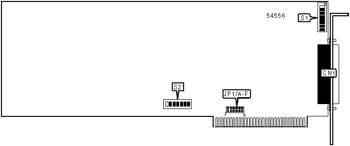
DB-37 connector |
CN1 |
|
USER CONFIGURABLE SETTINGS |
||
|
Function |
Label |
Position |
|
Channel 0 single-ended |
S1/0 |
Off |
|
Channel 0 differential |
S1/0 |
On |
|
Channel 1 single-ended |
S1/1 |
Off |
|
Channel 1 differential |
S1/1 |
On |
|
Channel 2 single-ended |
S1/2 |
Off |
|
Channel 2 differential |
S1/2 |
On |
|
Channel 3 single-ended |
S1/3 |
Off |
|
Channel 3 single-ended |
S1/3 |
On |
|
Channel 4 differential |
S1/4 |
Off |
|
Channel 4 single-ended |
S1/4 |
On |
|
Channel 5 differential |
S1/5 |
Off |
|
Channel 5 single-ended |
S1/5 |
On |
|
Channel 6 differential |
S1/6 |
Off |
|
Channel 6 single-ended |
S1/6 |
On |
|
Channel 7 differential |
S1/7 |
Off |
|
Channel 7 differential |
S1/7 |
On |
|
IRQ SELECTION |
||||||
|
Interrupt |
JP1/A |
JP1/B |
JP1/C |
JP1/D |
JP1/E |
JP1/F |
|
IRQ2 |
Closed |
Open |
Open |
Open |
Open |
Open |
|
IRQ3 |
Open |
Closed |
Open |
Open |
Open |
Open |
|
IRQ4 |
Open |
Open |
Closed |
Open |
Open |
Open |
|
IRQ5 |
Open |
Open |
Open |
Closed |
Open |
Open |
|
IRQ6 |
Open |
Open |
Open |
Open |
Closed |
Open |
|
IRQ7 |
Open |
Open |
Open |
Open |
Open |
Closed |
|
BASE I/O ADDRESS SELECTION |
||||||||
|
Setting |
S2/1 |
S2/2 |
S2/3 |
S2/4 |
S2/5 |
S2/6 |
S2/7 |
|
|
|
000h |
On |
On |
On |
On |
On |
On |
On |
|
|
018h |
Off |
Off |
On |
On |
On |
On |
On |
|
|
038h |
Off |
Off |
Off |
On |
On |
On |
Off |
|
|
100h |
On |
On |
On |
On |
On |
Off |
On |
|
|
200h |
On |
On |
On |
On |
On |
On |
Off |
|
» |
300h |
On |
On |
On |
On |
On |
Off |
Off |
|
|
380h |
On |
On |
On |
On |
Off |
Off |
Off |
|
|
3C0h |
On |
On |
On |
Off |
Off |
Off |
Off |
|
|
3E0h |
On |
On |
Off |
Off |
Off |
Off |
Off |
|
|
3F0h |
On |
Off |
Off |
Off |
Off |
Off |
Off |
|
|
3F8h |
Off |
Off |
Off |
Off |
Off |
Off |
Off |
|
Note: A total of 128 base address settings are available. The switches are a binary representation of the decimal memory addresses. S2/7 is the Most Significant Bit and switch S2/1 is the Least Significant Bit. The switches have the following decimal values: S2/7=512, S2/6=256, S2/5=128, S2/4=64, S2/3=32, S2/2=16, S2/1=8. Turn off the switches and add the values of the switches to obtain the correct memory address. (Off=1, On=0) |
||||||||