NATIONAL INSTRUMENTS
AT-A2150
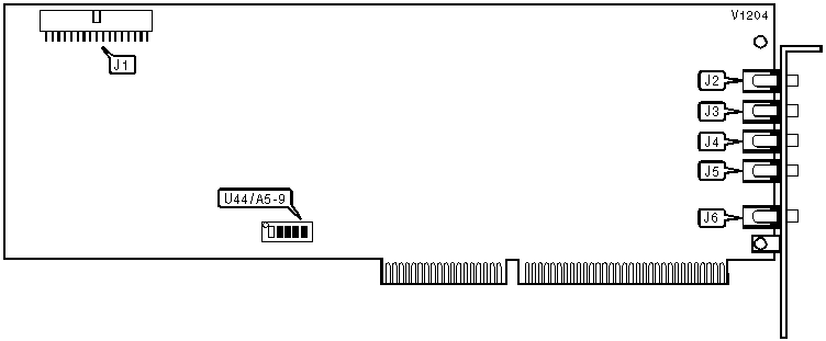
|
Card Type |
Dynamic signal acquisition converter |
|
Chipset Controller |
Unidentified |
|
I/O Options |
Analog input, analog output |
|
Maximum DRAM |
N/A |
|
CONNECTIONS | |||
|
Purpose |
Location |
Purpose |
Location |
|
34-pin interface connector |
J1 |
Analog input or output jack |
J4 |
|
Analog input or output jack |
J2 |
Analog input or output jack |
J5 |
|
Analog input or output jack |
J3 |
Analog input or output jack |
J6 |
|
Note: Exact function of each jack is unidentified. | |||
|
BASE I/O ADDRESS SELECTION | ||||||
|
Address |
U44/A5 |
U44/A6 |
U44/A7 |
U44/A8 |
U44/A9 | |
| » |
120h |
Off |
On |
On |
Off |
On |
|
000h |
On |
On |
On |
On |
On | |
|
020h |
Off |
On |
On |
On |
On | |
|
040h |
On |
Off |
On |
On |
On | |
|
060h |
Off |
Off |
On |
On |
On | |
|
080h |
On |
On |
Off |
On |
On | |
|
360h |
Off |
Off |
On |
Off |
Off | |
|
380h |
On |
On |
Off |
Off |
Off | |
|
3A0h |
Off |
On |
Off |
Off |
Off | |
|
3C0h |
On |
Off |
Off |
Off |
Off | |
|
3E0h |
Off |
Off |
Off |
Off |
Off | |
|
Note: A total of 255 base address settings are available. The switches are a binary representation of the decimal memory addresses. Switch A9 is the Most Significant Bit and switch A5 is the Least Significant Bit. The switches have the following decimal values: switch A9=512, A8=256, A7=128, A6=64, A5=32. Turn off the switches and add the values of the switches that are off to obtain the correct memory address. (Off=1, On=0) | ||||||