QUATECH, INC.
MPA-100
|
Card Type |
I/O controller |
|
Chipset/Controller |
AMD |
|
I/O Options |
Serial port |
|
Maximum DRAM |
N/A |
|
CONNECTIONS | |
|
Purpose |
Location |
|
Serial port |
CN1 |
|
CLOCK SPEED SELECT | ||
|
Speed |
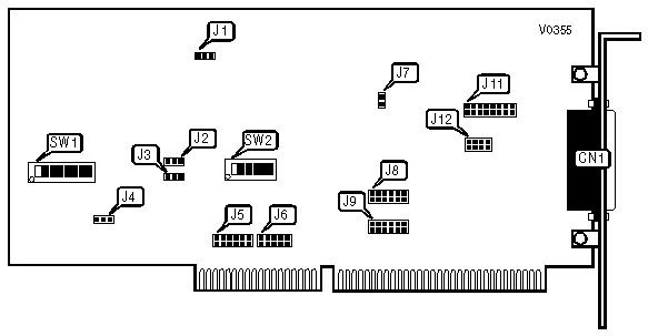
J1 | |
| » |
8MHz |
Pins 1 & 2 closed |
|
6MHz |
Pins 2 & 3 closed | |
|
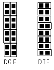
SERIAL PORT DTE/DCE CONFIGURATION |
|
Serial Port CN1 |
|
Jumper J11
|
|
SERIAL PORT DTE/DCE CONFIGURATION (CONTINUED) | |
|
Setting |
J2 |
|
DTE |
Closed |
|
DCE |
Open |
|
SERIAL PORT DTE/DCE CONFIGURATION (CONTINUED) | |
|
Setting |
J12 |
|
DTE |
Pins 1 & 5, 2 & 6, 3 & 7, 4 & 8 closed |
|
DCE |
Pins 1 & 2, 3 & 4, 5 & 6, 7 & 8 closed |
|
INTERRUPT CONFIGURATION | |
|
Setting |
J4 |
|
Interrupt Sharing |
Pins 1 & 2 closed |
|
No Interrupt Sharing |
Pins 2 & 3 closed |
|
INTERRUPT SELECT | ||
|
IRQ |
J5 |
J6 |
|
IRQ2 |
Pins 1 & 7 closed |
N/A |
|
IRQ3 |
Pins 2 & 8 closed |
N/A |
|
IRQ4 |
Pins 3 & 9 closed |
N/A |
|
IRQ5 |
Pins 4 & 10 closed |
N/A |
|
IRQ6 |
Pins 5 & 11 closed |
N/A |
|
IRQ7 |
Pins 6 & 12 closed |
N/A |
|
IRQ10 |
N/A |
Pins 1 & 6 closed |
|
IRQ11 |
N/A |
Pins 2 & 7 closed |
|
IRQ12 |
N/A |
Pins 3 & 8 closed |
|
IRQ14 |
N/A |
Pins 4 & 9 closed |
|
IRQ15 |
N/A |
Pins 5 & 10 closed |
|
DMA CHANNEL ON TRANSMIT SELECT | |
|
DMA Channel |
J8 |
|
1 |
Pins 1 & 7, 2 & 8 closed |
|
2 |
Pins 3 & 9, 4 & 10 closed |
|
3 |
Pins 5 & 11, 6 & 12 closed |
|
DMA CHANNEL ON RECEIVE SELECT | |
|
DMA Channel |
J9 |
|
1 |
Pins 1 & 7, 2 & 8 closed |
|
2 |
Pins 3 & 9, 4 & 10 closed |
|
3 |
Pins 5 & 11, 6 & 12 closed |
|
SYNCA/RLEN CONFIGURATION | |
|
Setting |
J7 |
|
SYNCA |
Closed |
|
RLEN |
Open |
|
I/O ADDRESS CONFIGURATION | ||
|
Address |
SW1 |
SW2 |
|
300h |
1 & 2, 3 & 4, 5 & 6 on |
1 & 2, 3 & 4, 5 & 6 on |
|
3F8h |
1 & 2, 3 & 4, 5 & 6 on |
All Off |
|
Note:The address range for the MPA-100 is from 0 to FFFFh. The switches are a binary representation of the addresses. The switches have the following decimal values: SW1/1=8, SW1/2=4, SW1/3=2, SW1/4=1, SW1/5=8, SW1/6=4, SW1/7=2, SW1/8=1, SW2/1=8, SW2/2=4, SW2/3=2, SW2/4=1, SW2/4=8. SW2/6 is unused. | ||
|
FACTORY CONFIGURED SETTINGS | |
|
Jumper |
Setting |
|
J3 |
N/A |