TANDON CORPORATION
QUAD SERIAL OPTION BOARD
|
Category |
I/O |
|
Data Bus Type |
8-bit ISA |
|
Memory Type |
Unidentified |
|
Maximum Onboard Memory |
Unidentified |
|
CONNECTIONS | |
|
Purpose |
Location |
|
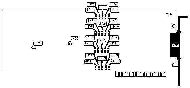
37-pin multi serial connector |
CN1 |
|
DSR CONTROL SETTINGS (CHANNEL 1) | |
|
Setting |
JP1 |
|
DSR controlled by driver |
Pins 1 & 2 closed |
|
DSR forced true |
Pins 2 & 3 closed |
|
DSR forced false |
All open |
|
DCD CONTROL SETTINGS (CHANNEL 1) | |
|
Setting |
JP2 |
|
DCD controlled by driver |
Pins 1 & 2 closed |
|
DCD forced true |
Pins 2 & 3 closed |
|
DCD forced false |
All open |
|
CTS CONTROL SETTINGS (CHANNEL 1) | |
|
Setting |
JP3 |
|
CTS controlled by driver |
Pins 1 & 2 closed |
|
CTS forced true |
Pins 2 & 3 closed |
|
CTS forced false |
All open |
|
DTR CONTROL SETTINGS (CHANNEL 1) | |
|
Setting |
JP4 |
|
DTR controlled by driver |
Pins 1 & 2 closed |
|
DTR forced true |
Pins 2 & 3 closed |
|
DTR forced false |
All open |
|
RTS CONTROL SETTINGS (CHANNEL 1) | |
|
Setting |
JP5 |
|
RTS controlled by driver |
Pins 1 & 2 closed |
|
RTS forced true |
Pins 2 & 3 closed |
|
RTS forced false |
All open |
|
DSR CONTROL SETTINGS (CHANNEL 2) | |
|
Setting |
JP6 |
|
DSR controlled by driver |
Pins 1 & 2 closed |
|
DSR forced true |
Pins 2 & 3 closed |
|
DSR forced false |
All open |
|
DCD CONTROL SETTINGS (CHANNEL 2) | |
|
Setting |
JP7 |
|
DCD controlled by driver |
Pins 1 & 2 closed |
|
DCD forced true |
Pins 2 & 3 closed |
|
DCD forced false |
All open |
|
CTS CONTROL SETTINGS (CHANNEL 2) | |
|
Setting |
JP8 |
|
CTS controlled by driver |
Pins 1 & 2 closed |
|
CTS forced true |
Pins 2 & 3 closed |
|
CTS forced false |
All open |
|
DTR CONTROL SETTINGS (CHANNEL 2) | |
|
Setting |
JP9 |
|
DTR controlled by driver |
Pins 1 & 2 closed |
|
DTR forced true |
Pins 2 & 3 closed |
|
DTR forced false |
All open |
|
RTS CONTROL SETTINGS (CHANNEL 2) | |
|
Setting |
JP10 |
|
RTS controlled by driver |
Pins 1 & 2 closed |
|
RTS forced true |
Pins 2 & 3 closed |
|
RTS forced false |
All open |
|
DSR CONTROL SETTINGS (CHANNEL 3) | |
|
Setting |
JP11 |
|
DSR controlled by driver |
Pins 1 & 2 closed |
|
DSR forced true |
Pins 2 & 3 closed |
|
DSR forced false |
All open |
|
DCD CONTROL SETTINGS (CHANNEL 3) | |
|
Setting |
JP12 |
|
DCD controlled by driver |
Pins 1 & 2 closed |
|
DCD forced true |
Pins 2 & 3 closed |
|
DCD forced false |
All open |
|
CTS CONTROL SETTINGS (CHANNEL 3) | |
|
Setting |
JP13 |
|
CTS controlled by driver |
Pins 1 & 2 closed |
|
CTS forced true |
Pins 2 & 3 closed |
|
CTS forced false |
All open |
|
DTR CONTROL SETTINGS (CHANNEL 3) | |
|
Setting |
JP14 |
|
DTR controlled by driver |
Pins 1 & 2 closed |
|
DTR forced true |
Pins 2 & 3 closed |
|
DTR forced false |
All open |
|
RTS CONTROL SETTINGS (CHANNEL 3) | |
|
Setting |
JP15 |
|
RTS controlled by driver |
Pins 1 & 2 closed |
|
RTS forced true |
Pins 2 & 3 closed |
|
RTS forced false |
All open |
|
DSR CONTROL SETTINGS (CHANNEL 4) | |
|
Setting |
JP16 |
|
DSR controlled by driver |
Pins 1 & 2 closed |
|
DSR forced true |
Pins 2 & 3 closed |
|
DSR forced false |
All open |
|
DCD CONTROL SETTINGS (CHANNEL 4) | |
|
Setting |
JP17 |
|
DCD controlled by driver |
Pins 1 & 2 closed |
|
DCD forced true |
Pins 2 & 3 closed |
|
DCD forced false |
All open |
|
CTS CONTROL SETTINGS (CHANNEL 4) | |
|
Setting |
JP18 |
|
CTS controlled by driver |
Pins 1 & 2 closed |
|
CTS forced true |
Pins 2 & 3 closed |
|
CTS forced false |
All open |
|
DTR CONTROL SETTINGS (CHANNEL 4) | |
|
Setting |
JP19 |
|
DTR controlled by driver |
Pins 1 & 2 closed |
|
DTR forced true |
Pins 2 & 3 closed |
|
DTR forced false |
All open |
|
RTS CONTROL SETTINGS (CHANNEL 4) | |
|
Setting |
JP20 |
|
RTS controlled by driver |
Pins 1 & 2 closed |
|
RTS forced true |
Pins 2 & 3 closed |
|
RTS forced false |
All open |
|
BOARD NUMBER SETTINGS | ||
|
Address |
JP21 |
JP22 |
|
Primary board 1 |
Pins 1 & 2 closed |
Pins 1 & 2 closed |
|
Secondary board 2 |
Pins 2 & 3 closed |
Pins 2 & 3 closed |
|
TWO BOARD ADDRESSING | |
|
Primary Board |
Secondary Board |
|
280-287h = Port 1A |
2A0-2A7h = Port 2A |
|
288-28Fh = Port 1B |
2A8-2AFh = Port 2B |
|
290-297h = Port 1C |
2B0-2B8h = Port 2C |
|
298-29Fh = Port 1D |
2B8-2BFh = Port 2D |