ASUS COMPUTER INTERNATIONAL
PCI/I-P54TP4
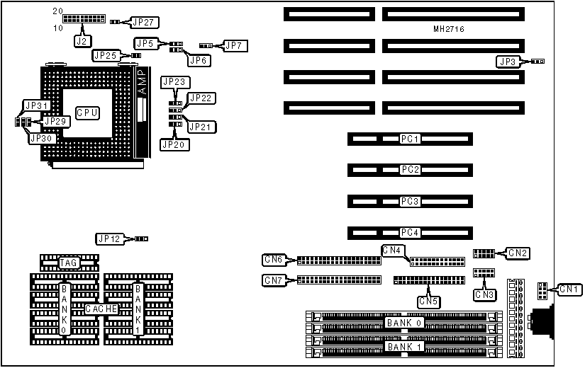
|
Processor |
Pentium |
|
Processor Speed |
75/90/100MHz |
|
Chip Set |
Unidentified |
|
Max. Onboard DRAM |
128MB |
|
Cache |
256/512KB |
|
BIOS |
Award |
|
Dimensions |
330mm x 218mm |
|
I/O Options |
32-bit PCI slots (4), floppy drive interface, green PC connector, IDE interfaces (2), parallel port, PS/2 mouse interface, serial ports (2) |
|
NPU Options |
None |
|
CONNECTIONS | |||
|
Purpose |
Location |
Purpose |
Location |
|
PS/2 mouse interface |
CN1 |
Power LED & keylock |
J2 pins 1 - 5 |
|
Serial port 1 |
CN2 |
Speaker |
J2 pins 7 - 10 |
|
Serial port 2 |
CN3 |
Turbo LED |
J2 pins 12 - 13 |
|
Parallel port |
CN4 |
Green PC connector |
J2 pins 14 - 15 |
|
Floppy drive interface |
CN5 |
Reset switch |
J2 pins 19 - 20 |
|
IDE interface (primary) |
CN6 |
IDE interface LED |
JP27 |
|
IDE interface (secondary) |
CN7 |
32-bit PCI slots |
PC1 - PC4 |
|
USER CONFIGURABLE SETTINGS | |||
|
Function |
Jumper |
Position | |
|
» |
On board I/O enabled |
JP3 |
pins 1 & 2 closed |
|
On board I/O disabled |
JP3 |
pins 2 & 3 closed | |
|
» |
PS/2 mouse enabled |
JP7 |
pins 1 & 2 closed |
|
PS/2 mouse disabled |
JP7 |
pins 2 & 3 closed | |
|
» |
CPU external clock speed select 1.5x |
JP25 |
Open |
|
CPU external clock speed select 2x |
JP25 |
Closed | |
|
DRAM CONFIGURATION | ||
|
Size |
Bank 0 |
Bank 1 |
|
8MB |
(2) 1M x 36 |
NONE |
|
8MB |
NONE |
(2) 1M x 36 |
|
16MB |
(2) 2M x 36 |
NONE |
|
16MB |
NONE |
(2) 2M x 36 |
|
16MB |
(2) 1M x 36 |
(2) 1M x 36 |
|
24MB |
(2) 1M x 36 |
(2) 2M x 36 |
|
24MB |
(2) 2M x 36 |
(2) 1M x 36 |
|
32MB |
(2) 4M x 36 |
NONE |
|
32MB |
NONE |
(2) 4M x 36 |
|
32MB |
(2) 2M x 36 |
(2) 2M x 36 |
|
40MB |
(2) 1M x 36 |
(2) 4M x 36 |
|
40MB |
(2) 4M x 36 |
(2) 1M x 36 |
|
48MB |
(2) 2M x 36 |
(2) 4M x 36 |
|
48MB |
(2) 4M x 36 |
(2) 2M x 36 |
|
64MB |
(2) 8M x 36 |
NONE |
|
64MB |
NONE |
(2) 8M x 36 |
|
64MB |
(2) 4M x 36 |
(2) 4M x 36 |
|
72MB |
(2) 1M x 36 |
(2) 8M x 36 |
|
72MB |
(2) 8M x 36 |
(2) 1M x 36 |
|
80MB |
(2) 2M x 36 |
(2) 8M x 36 |
|
80MB |
(2) 8M x 36 |
(2) 2M x 36 |
|
96MB |
(2) 4M x 36 |
(2) 8M x 36 |
|
96MB |
(2) 8M x 36 |
(2) 4M x 36 |
|
128MB |
(2) 8M x 36 |
(2) 8M x 36 |
|
CACHE CONFIGURATION | |||
|
Size |
Bank 0 |
Bank 1 |
TAG |
|
256KB |
(4) 32K x 8 |
(4) 32K x 8 |
(1) 8K x 8 or (1) 32K x 8 |
|
512KB |
(4) 64K x 8 |
(4) 64K x 8 |
(1) 32K x 8 |
|
CACHE JUMPER CONFIGURATION | |
|
Size |
JP12 |
|
256KB |
pins 2 & 3 closed |
|
512KB |
pins 1 & 2 closed |
|
CPU SPEED CONFIGURATION | ||||
|
Speed |
JP20 |
JP21 |
JP22 |
JP23 |
|
75MHz |
pins 1 & 2 closed |
pins 1 & 2 closed |
pins 1 & 2 closed |
pins 2 & 3 closed |
|
90MHz |
pins 2 & 3 closed |
pins 1 & 2 closed |
pins 2 & 3 closed |
pins 1 & 2 closed |
|
100MHz |
pins 2 & 3 closed |
pins 2 & 3 closed |
pins 1 & 2 closed |
pins 2 & 3 closed |
|
CPU VOLTAGE CONFIGURATION | |||
|
Voltage |
JP29 |
JP30 |
JP31 |
|
3.4v |
Closed |
Open |
Open |
|
3.5v |
Open |
Closed |
Open |
|
3.6v |
Open |
Open |
Closed |
|
BIOS CONFIGURATION | ||
|
Setting |
JP5 |
JP6 |
|
Flash BIOS programming disabled |
pins 1 & 2 closed |
pins 2 & 3 closed |
|
Flash BIOS programming enabled |
pins 2 & 3 closed |
pins 2 & 3 closed |