INTEL CORPORATION
ADVANCED/MN (MORRISSON)
|
Processor |
Pentium |
|
Processor Speed |
75/90/100/120MHz |
|
Chip Set |
Unidentified |
|
Max. Onboard DRAM |
128MB |
|
Cache |
256/512KB |
|
BIOS |
AMI |
|
Dimensions |
330mm x 218mm |
|
I/O Options |
PS/2 mouse port, parallel port, serial ports (2), VGA port, VGA feature connector, green PC connector, floppy drive interface, IDE interfaces (2) |
|
NPU Options |
None |
|
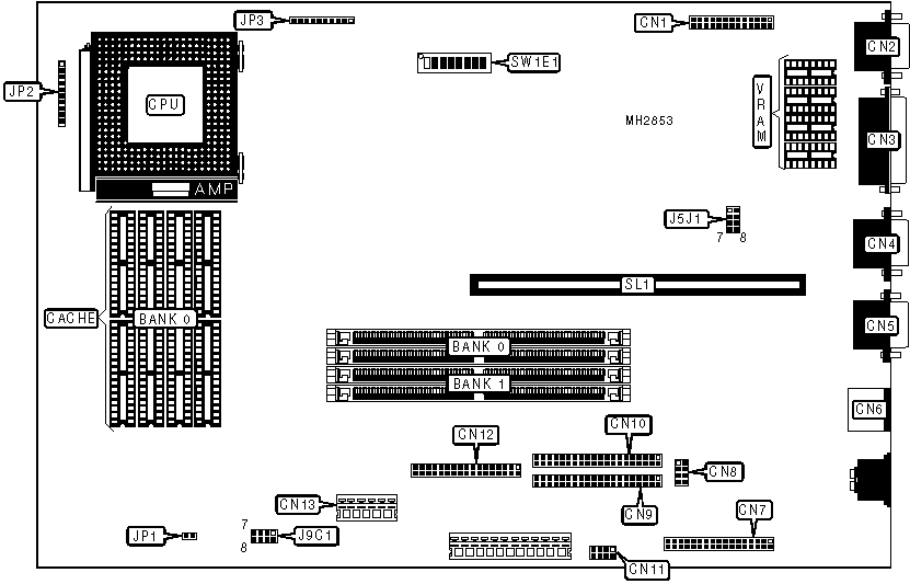
CONNECTIONS | |||
|
Purpose |
Location |
Purpose |
Location |
|
VGA feature connector |
CN1 |
IDE interface |
CN10 |
|
VGA port |
CN2 |
CD-ROM audio connector |
CN11 |
|
Parallel port |
CN3 |
Floppy drive interface |
CN12 |
|
Serial port 1 |
CN4 |
Power supply remote connector |
CN13 |
|
Serial port 2 |
CN5 |
Green PC connector |
JP1 |
|
PS/2 mouse port |
CN6 |
Front panel connector |
JP2 |
|
Audio I/O connector |
CN7 |
Front panel connector |
JP3 |
|
Wave table connector |
CN8 |
Riser Card |
SL1 |
|
IDE interface |
CN9 | ||
|
Note: The actual sizes of jumpers CN7, CN8, CN10, JP2, JP3 are unidentified. They are shown for location purposes only. | |||
|
USER CONFIGURABLE SETTINGS | |||
|
Function |
Jumper/Switch |
Position | |
|
» |
ISA clock speed select 1/6 |
J5J1 |
pins 5 & 7 open |
|
ISA clock speed select 1/8 |
J5J1 |
pins 5 & 7 closed | |
|
» |
Recovery boot enabled |
J5J1 |
pins 1 & 3 closed |
|
Recovery boot disabled |
J5J1 |
pins 1 & 2 closed | |
|
» |
CPU type select VR rated |
J9C1 |
pins 1 & 3 closed |
|
CPU type select VRE rated |
J9C1 |
pins 5 & 7 closed | |
|
» |
Password normal operation |
SW1E1/3 |
Off |
|
Password clear |
SW1E1/3 |
On | |
|
» |
CMOS memory normal operation |
SW1E1/4 |
Off |
|
CMOS memory clear |
SW1E1/4 |
On | |
|
» |
CMOS setup utility access enabled |
SW1E1/5 |
Off |
|
CMOS setup utility access disabled |
SW1E1/5 |
On | |
|
DRAM CONFIGURATION | ||
|
Size |
Bank 0 |
Bank 1 |
|
8MB |
(2) 1M x 36 |
NONE |
|
8MB |
NONE |
(2) 1M x 36 |
|
16MB |
(2) 2M x 36 |
NONE |
|
16MB |
NONE |
(2) 2M x 36 |
|
16MB |
(2) 1M x 36 |
(2) 1M x 36 |
|
24MB |
(2) 1M x 36 |
(2) 2M x 36 |
|
24MB |
(2) 2M x 36 |
(2) 1M x 36 |
|
32MB |
(2) 2M x 36 |
(2) 2M x 36 |
|
48MB |
(2) 2M x 36 |
(2) 4M x 36 |
|
48MB |
(2) 4M x 36 |
(2) 2M x 36 |
|
64MB |
(2) 4M x 36 |
(2) 4M x 36 |
|
72MB |
(2) 1M x 36 |
(2) 8M x 36 |
|
72MB |
(2) 8M x 36 |
(2) 1M x 36 |
|
128MB |
(2) 8M x 36 |
(2) 8M x 36 |
|
CACHE CONFIGURATION | |
|
Size |
Bank 0 |
|
256KB |
(8) 32K x 8 |
|
512KB |
(8) 64K x 8 |
|
CACHE JUMPER CONFIGURATION | ||
|
Size |
SW1E1/1 |
SW1E1/2 |
|
256KB |
Off |
Off |
|
512KB |
Off |
On |
|
CPU SPEED CONFIGURATION | |||
|
Speed |
SW1E1/6 |
SW1E1/7 |
SW1E1/8 |
|
75MHz |
Off |
Off |
Off |
|
90MHz |
Off |
On |
Off |
|
100MHz |
Off |
Off |
On |
|
120MHz |
On |
On |
Off |
|
VRAM CONFIGURATION |
|
VRAM is upgradable to 2MB, but the chip size is unidentified. |