MICRO-STAR INTERNATIONAL CO., LTD.
MS-4132G VLB 486 SI3G
|
Processor |
80486SX/80487SX/80486SX-SL/80486DX/80486DX-SL |
|
Processor Speed |
25/33/40/50MHz |
|
Chip Set |
SIS |
|
Max. Onboard DRAM |
32MB |
|
Cache |
128/256KB |
|
BIOS |
Phoenix |
|
Dimensions |
254mm x 218mm |
|
I/O Options |
32-Bit VESA local bus slots (3) |
|
NPU Options |
None |
|
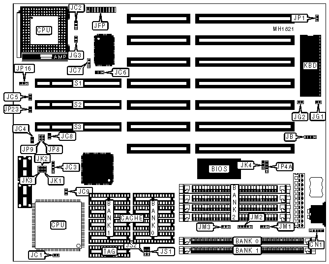
CONNECTIONS |
|||
|
Purpose |
Location |
Purpose |
Location |
|
Internal keyboard connector |
CN1 |
Power saving switch |
JG3 |
|
External battery |
JB |
32-Bit VESA local bus slot |
S1 |
|
Green Function |
JC7 |
32-Bit VESA local bus slot |
S2 |
|
Monitor power control |
JG1 |
32-Bit VESA local bus slot |
S3 |
|
Green PC LED |
JG2 |
|
|
|
PIN OUT CONFIGURATION |
|
|
Connector |
JFP |
|
Keylock |
pins 1 & 2 closed |
|
Power LED |
pins 3 & 5 closed |
|
Turbo LED |
pins 12 & 13 closed |
|
Turbo switch |
pins 15, 16, & 17 closed |
|
Reset |
pins 19 & 20 closed |
|
Speaker |
pins 7, 8, 9, & 10 closed |
|
USER CONFIGURABLE SETTINGS |
|||
|
Function |
Jumper |
Position |
|
|
» |
CPU PQFP not installed |
JC1 |
Closed |
|
|
CPU PQFP installed |
JC1 |
Open |
|
» |
Monitor type select monochrome |
JP1 |
Open |
|
|
Monitor type select color |
JP1 |
Closed |
|
» |
Factory configured - do not alter |
JP4A |
pins 1 & 2 closed |
|
» |
Factory configured - do not alter |
JP16 |
N/A |
|
» |
Normal VL-bus card installed |
JP23 |
Open |
|
|
Special VL-bus card installed |
JP23 |
Closed |
|
CACHE CONFIGURATION |
|||
|
Size |
Bank 0 |
Bank 1 |
TAG |
|
128KB |
(4) 32K x 8 |
NONE |
(1) 8K x 8 |
|
256KB |
(4) 32K x 8 |
(4) 32K x 8 |
(1) 32K x 8 |
|
CACHE JUMPER CONFIGURATION |
||
|
Size |
JS1 |
JS2 |
|
128KB |
pins 1 & 2 closed |
pins 1 & 2 closed |
|
256KB |
pins 2 & 3 closed |
pins 2 & 3 closed |
|
CPU TYPE CONFIGURATION |
|||||||
|
Type |
JC2 |
JC3 |
JC4 |
JC5 |
JC6 |
JC8 |
JC9 |
|
80486SX |
Open |
pins 2 & 3 |
N/A |
N/A |
Open |
Closed |
Closed |
|
80486SX-SL |
pins 2 & 3 |
pins 2 & 3 |
pins 1 & 2 |
pins 1 & 2 |
Open |
Closed |
Closed |
|
80487SX |
Open |
1 & 2, 3 & 4 |
N/A |
N/A |
pins 1 & 2 |
Open |
Open |
|
80486DX |
Open |
1 & 2, 3 & 4 |
N/A |
N/A |
pins 2 & 3 |
Open |
Open |
|
80486DX-SL |
pins 2 & 3 |
1 & 2, 3 & 4 |
pins 1 & 2 |
pins 1 & 2 |
pins 2 & 3 |
Closed |
Closed |
|
Note:Pins designated should be in the closed position. |
|||||||
|
VESA WAIT STATE/BUS SPEED CONFIGURATION |
|||
|
Speed |
Wait states |
JP8 |
JP9 |
|
< 33MHz |
0 wait states |
Open |
Open |
|
> 33MHz |
1 wait state |
Closed |
Closed |
|
CPU SPEED CONFIGURATION |
||||
|
Speed |
JK1 |
JK2 |
JK3 |
JK4 |
|
25MHz |
Open |
Open |
Closed |
pins 2 & 3 closed |
|
33MHz |
Closed |
Open |
Open |
pins 2 & 3 closed |
|
40MHz |
Closed |
Closed |
Open |
pins 2 & 3 closed |
|
50MHz |
Open |
Closed |
Open |
pins 1 & 2 closed |
|
DRAM BANK AND JUMPER CONFIGURATION |
||||||
|
Size |
Bank 0 |
Bank 1 |
Bank 2 |
JM1 |
JM2 |
JM3 |
|
4MB |
(1) 256KB x 36 DS |
(1) 512KB x 36 |
NONE |
1 & 2 |
N/A |
N/A |
|
4MB |
(1) 256K x 36 |
(1) 512KB x 36 |
(4) 256K x 9 |
1 & 2 |
4 & 5 |
1 & 2 |
|
4MB |
(1) 512KB x 36 |
(1) 512KB x 36 |
NONE |
2 & 3 |
N/A |
N/A |
|
4MB |
(1) 1M x 36 |
NONE |
NONE |
N/A |
N/A |
N/A |
|
4MB |
NONE |
NONE |
(4) 1M x 9 |
N/A |
N/A |
2 & 3 |
|
8MB |
(1) 256KB x 36 DS |
(1) 512KB x 36 |
(4) 1M x 9 |
1 & 2 |
1 & 2 |
1 & 2 |
|
8MB |
(1) 256KB x 36 DS |
(1) 1M x 36 |
NONE |
1 & 2 |
N/A |
N/A |
|
8MB |
(1) 256KB x 36 DS |
NONE |
(4) 1M x 9 |
N/A |
2 & 3 |
1 & 2 |
|
8MB |
(1) 1M x 36 |
(1) 1M x 36 |
NONE |
2 & 3 |
N/A |
N/A |
|
8MB |
(1) 1M x 36 |
NONE |
(4) 1M x 9 |
N/A |
4 & 5 |
1 & 2 |
|
8MB |
(1) 1M x 36 DS |
NONE |
NONE |
N/A |
N/A |
N/A |
|
12MB |
(1) 256KB x 36 DS |
(1) 1M x 36 |
(4) 1M x 9 |
1 & 2 |
1 & 2 |
1 & 2 |
|
12MB |
(1) 1M x 36 |
(1) 1M x 36 |
(4) 1M x 9 |
1 & 2 |
4 & 5 |
1 & 2 |
|
16MB |
(1) 1M x 36 DS |
(1) 1M x 36 |
(4) 1M x 9 |
1 & 2 |
1 & 2 |
1 & 2 |
|
16MB |
(1) 1M x 36 DS |
(1) 1M x 36 DS |
NONE |
1 & 2 |
1 & 2 |
1 & 2 |
|
16MB |
(1) 4M x 36 |
NONE |
NONE |
N/A |
N/A |
N/A |
|
16MB |
NONE |
NONE |
(4) 4M x 9 |
N/A |
N/A |
2 & 3 |
|
20MB |
(1) 2M x 36 |
(1) 2M x 36 |
(4) 4M x 9 |
2 & 3 |
2 & 3 |
1 & 2 |
|
24MB |
(1) 2M x 36 DS |
(1) 4M x 36 |
(4) 4M x 9 |
1 & 2 |
1 & 2 |
1 & 2 |
|
32MB |
(1) 4M x 36 |
(1) 4M x 36 |
NONE |
2 & 3 |
N/A |
N/A |
|
64MB |
(1) 4M x 36 DS |
(1) 4M x 36 DS |
NONE |
1 & 2 |
1 & 2 |
1 & 2 |
|
64MB |
(1) 4M x 36 DS |
(1) 4M x 36 |
(4) 4M x 9 |
1 & 2 |
1 & 2 |
1 & 2 |
|
Note:Pins designated should be in the closed position. |
||||||