SEANIX TECHNOLOGY, INC.
ASI 9000
|
Processor |
AM K5/CXM1/Pentium |
|
Processor Speed |
75/90/100/120/133MHz |
|
Chip Set |
OPTI |
|
Max. Onboard DRAM |
128MB |
|
Cache |
256/512/1024/2048KB |
|
BIOS |
Award |
|
Dimensions |
330mm x 218mm |
|
I/O Options |
32-bit PCI slots (3), floppy drive interface, IDE interfaces (2), parallel port, serial ports (2), cache slot |
|
NPU Options |
None |
|
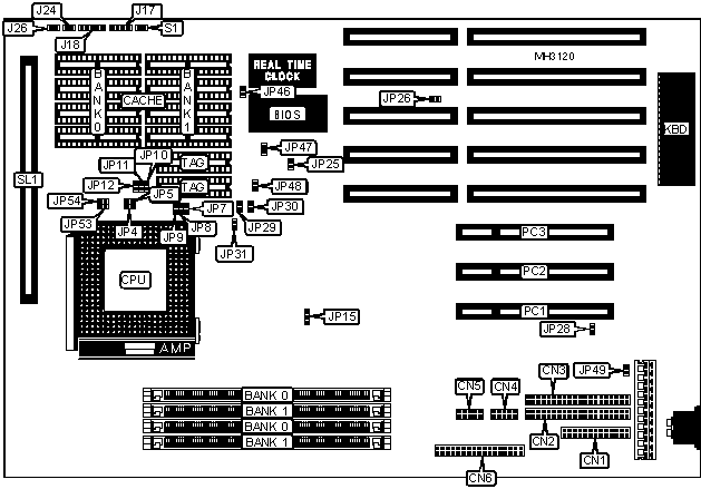
CONNECTIONS | |||
|
Purpose |
Location |
Purpose |
Location |
|
Parallel port |
CN1 |
Speaker |
J17 |
|
IDE interface 2 |
CN2 |
Power LED & keylock |
J18 |
|
IDE interface 1 |
CN3 |
32-bit PCI slots |
PC1 - PC3 |
|
Serial port 1 |
CN4 |
Reset switch |
S1 |
|
Serial port 2 |
CN5 |
Cache slot |
SL1 |
|
Floppy drive interface |
CN6 | ||
|
USER CONFIGURABLE SETTINGS | |||
|
Function |
Jumper |
Position | |
|
» |
Factory configured - do not alter |
J24 |
N/A |
|
» |
Factory configured - do not alter |
J26 |
N/A |
|
BIOS voltage select 12v |
JP15 |
pins 1 & 2 closed | |
|
BIOS voltage select 5v |
JP15 |
pins 2 & 3 closed | |
|
» |
Factory configured - do not alter |
JP25 |
N/A |
|
» |
Factory configured - do not alter |
JP26 |
N/A |
|
» |
Factory configured - do not alter |
JP28 |
N/A |
|
» |
CMOS memory normal operation |
JP46 |
Open |
|
CMOS memory clear |
JP46 |
Closed | |
|
» |
Factory configured - do not alter |
JP47 |
N/A |
|
» |
Factory configured - do not alter |
JP48 |
N/A |
|
IDE select primary and secondary |
JP49 |
pins 1 & 2 closed | |
|
IDE select primary only |
JP49 |
pins 2 & 3 closed | |
|
IDE interface enabled |
JP55 |
Closed | |
|
IDE interface disabled |
JP55 |
Open | |
|
Note: The location of JP55 is unidentified. | |||
|
DRAM CONFIGURATION | ||
|
Size |
Bank 0 |
Bank 1 |
|
2MB |
(2) 256K x 36 |
NONE |
|
4MB |
(2) 512K x 36 |
NONE |
|
4MB |
(2) 256K x 36 |
(2) 256K x 36 |
|
6MB |
(2) 512K x 36 |
(2) 256K x 36 |
|
6MB |
(2) 256K x 36 |
(2) 512K x 36 |
|
8MB |
(2) 1M x 36 |
NONE |
|
8MB |
(2) 512K x 36 |
(2) 512K x 36 |
|
10MB |
(2) 1M x 36 |
(2) 256K x 36 |
|
10MB |
(2) 256K x 36 |
(2) 1M x 36 |
|
12MB |
(2) 1M x 36 |
(2) 512K x 36 |
|
12MB |
(2) 512K x 36 |
(2) 1M x 36 |
|
16MB |
(2) 2M x 36 |
NONE |
|
16MB |
(2) 1M x 36 |
(2) 1M x 36 |
|
18MB |
(2) 2M x 36 |
(2) 256K x 36 |
|
18MB |
(2) 256K x 36 |
(2) 2M x 36 |
|
20MB |
(2) 2M x 36 |
(2) 512K x 36 |
|
20MB |
(2) 512K x 36 |
(2) 2M x 36 |
|
24MB |
(2) 2M x 36 |
(2) 1M x 36 |
|
24MB |
(2) 1M x 36 |
(2) 2M x 36 |
|
32MB |
(2) 4M x 36 |
NONE |
|
32MB |
(2) 2M x 36 |
(2) 2M x 36 |
|
34MB |
(2) 4M x 36 |
(2) 256K x 36 |
|
34MB |
(2) 256K x 36 |
(2) 4M x 36 |
|
36MB |
(2) 4M x 36 |
(2) 512K x 36 |
|
36MB |
(2) 512K x 36 |
(2) 4M x 36 |
|
DRAM CONFIGURATION (CON’T) | ||
|
Size |
Bank 0 |
Bank 1 |
|
40MB |
(2) 4M x 36 |
(2) 1M x 36 |
|
40MB |
(2) 1M x 36 |
(2) 4M x 36 |
|
48MB |
(2) 4M x 36 |
(2) 2M x 36 |
|
48MB |
(2) 2M x 36 |
(2) 4M x 36 |
|
64MB |
(2) 8M x 36 |
NONE |
|
64MB |
(2) 4M x 36 |
(2) 4M x 36 |
|
66MB |
(2) 8M x 36 |
(2) 256K x 36 |
|
66MB |
(2) 256K x 36 |
(2) 8M x 36 |
|
68MB |
(2) 8M x 36 |
(2) 512K x 36 |
|
68MB |
(2) 512K x 36 |
(2) 8M x 36 |
|
72MB |
(2) 8M x 36 |
(2) 1M x 36 |
|
72MB |
(2) 1M x 36 |
(2) 8M x 36 |
|
80MB |
(2) 8M x 36 |
(2) 2M x 36 |
|
80MB |
(2) 2M x 36 |
(2) 8M x 36 |
|
96MB |
(2) 8M x 36 |
(2) 4M x 36 |
|
96MB |
(2) 4M x 36 |
(2) 8M x 36 |
|
128MB |
(2) 8M x 36 |
(2) 8M x 36 |
|
DRAM JUMPER CONFIGURATION | ||
|
Size |
JP4 |
JP5 |
|
512KB <= 64MB |
Open |
Closed |
|
512KB > 64MB |
Open |
Closed |
|
256KB <= 32MB |
Open |
Open |
|
256KB > 32MB |
Open |
Open |
|
1MB |
Closed |
Closed |
|
CACHE CONFIGURATION | ||||
|
Size |
Bank 0 |
Bank 1 |
TAG |
SL1 |
|
256KB (A) |
(4) 32K x 8 |
(4) 32K x 8 |
(1) 32K x 8 |
Not installed |
|
256KB (B) |
NONE |
NONE |
(1) 32K x 8 |
Installed |
|
512KB (A) |
(4) 64K x 8 |
(4) 64K x 8 |
(1) 32K x 8 |
Not installed |
|
512KB (B) |
NONE |
NONE |
(1) 32K x 8 |
Installed |
|
1MB (A) |
(4) 128K x 8 |
(4) 128K x 8 |
(1) 32K x 8 |
Not installed |
|
1MB (B) |
NONE |
NONE |
(1) 32K x 8 |
Installed |
|
2MB |
NONE |
NONE |
(1) 32K x 8 |
Installed |
|
CACHE VOLTAGE CONFIGURATION | ||||||
|
Voltage |
JP7 |
JP8 |
JP9 |
JP10 |
JP11 |
JP12 |
|
3.3v |
Open |
Open |
Open |
Closed |
Closed |
Open |
|
5v |
Closed |
Closed |
Closed |
Open |
Open |
Closed |
|
CPU SPEED CONFIGURATION | |||||
|
Speed |
JP29 |
JP30 |
JP31 |
JP53 |
JP54 |
|
75MHz |
Open |
Open |
Open |
Open |
pins 1 & 2 closed |
|
90MHz |
Closed |
Closed |
Open |
Open |
pins 1 & 2 closed |
|
100MHz |
Closed |
Open |
Open |
Open |
pins 1 & 2 closed |
|
120MHz |
Closed |
Closed |
Open |
Open |
pins 2 & 3 closed |
|
133MHz |
Closed |
Open |
Open |
Open |
pins 2 & 3 closed |
|
MISCELLANEOUS TECHNICAL NOTE |
|
Note: The location of pin 1 is unidentified. |