SEANIX TECHNOLOGY, INC.
YUKON SYSTEM BOARD
|
Processor |
Pentium |
|
Processor Speed |
75/90/100/120/133MHz |
|
Chip Set |
SIS |
|
Maximum Onboard Memory |
128MB |
|
Cache |
256/512/1024KB |
|
BIOS |
Award |
|
Dimensions |
330mm x 218mm |
|
I/O Options |
32-bit PCI slots (4), floppy drive interface, IDE interfaces (2), parallel port, serial port, serial port/IRDA, VGA feature connector, VRM connector, cache slot, IR connector, VGA - TV - PS/2 out connector, audio - MIDI connector, CD-ROM audio cable connector, wavetable connector |
|
NPU Options |
None |
|
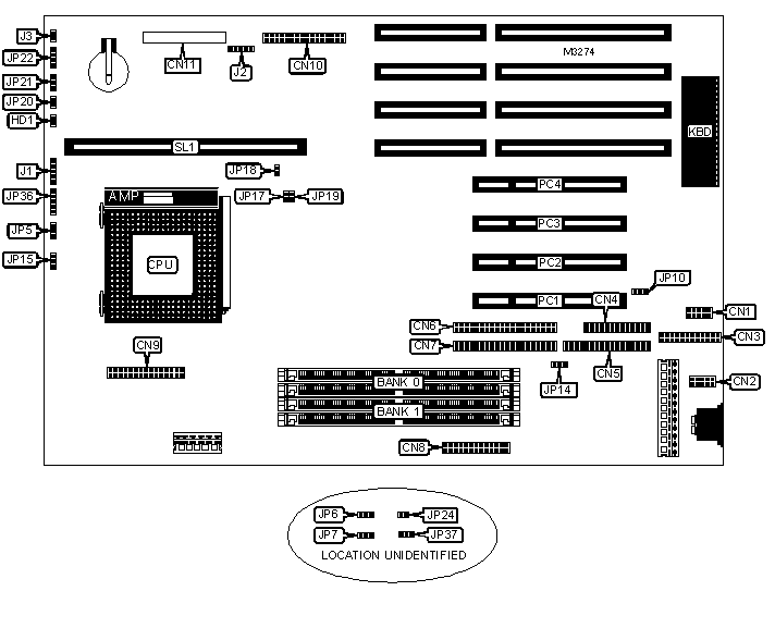
CONNECTIONS | |||
|
Function |
Label |
Function |
Label |
|
Serial port 2/IRDA |
CN1 |
IDE interface LED |
HD1 |
|
Serial port 1 |
CN2 |
Power LED & keylock |
J1 |
|
VGA - TV - PS/2 out connector |
CN3 |
CD-ROM audio connector |
J2 |
|
Parallel port |
CN4 |
Reset switch |
J3 |
|
Floppy drive interface |
CN5 |
Turbo LED |
JP20 |
|
IDE interface 1 |
CN6 |
Turbo switch |
JP21 |
|
IDE interface 2 |
CN7 |
Speaker |
JP22 |
|
VGA feature connector |
CN8 |
IR connector |
JP36 |
|
VRM connector |
CN9 |
32-bit PCI slots |
PC1 - PC4 |
|
Audio/MIDI cable connector |
CN10 |
Cache slot |
SL1 |
|
Wavetable upgrade connector |
CN11 | ||
|
USER CONFIGURABLE SETTINGS | |||
|
Setting |
Label |
Position | |
|
» |
L1 cache always invalidated |
JP5 |
Pins 1 & 2 closed |
|
L1 cache invalidated on write only |
JP5 |
Pins 2 & 3 closed | |
|
» |
Serial port 2 used for IRDA |
JP10 |
Pins 1 & 2 closed |
|
Serial port 2 used for COM2 |
JP10 |
Pins 2 & 3 closed | |
|
» |
Pipeline mode enabled |
JP14 |
Pins 2 & 3 closed |
|
Pipeline mode disabled |
JP14 |
Pins 1 & 2 closed | |
|
» |
Cache type select asynchronous |
JP15 |
Pins 1 & 2 closed |
|
Cache type select synchronous |
JP15 |
Pins 2 & 3 closed | |
|
» |
PCI bus clock speed select 33MHz |
JP18 |
Open |
|
PCI bus clock speed select CPUCLK/2 |
JP18 |
Closed | |
|
» |
VGA shared memory enabled |
JP24 |
Closed |
|
VGA shared memory disabled |
JP24 |
Open | |
|
» |
Parallel port IRQ select IRQ7 |
JP37 |
Pins 1 & 2 closed |
|
Parallel port IRQ select IRQ5 |
JP37 |
Pins 2 & 3 closed | |
|
Note: The location of jumpers JP24 & JP37 are unidentified. | |||
|
DRAM | ||
|
Size |
Bank 0 |
Bank 1 |
|
2MB |
(2) 256K x 36 |
None |
|
4MB |
(2) 512K x 36 |
None |
|
4MB |
(2) 256K x 36 |
(2) 256K x 36 |
|
6MB |
(2) 256K x 36 |
(2) 512K x 36 |
|
8MB |
(2) 1M x 36 |
None |
|
8MB |
(2) 512K x 36 |
(2) 512K x 36 |
|
10MB |
(2) 256K x 36 |
(2) 1M x 36 |
|
12MB |
(2) 512K x 36 |
(2) 1M x 36 |
|
16MB |
(2) 2M x 36 |
None |
|
16MB |
(2) 1M x 36 |
(2) 1M x 36 |
|
DRAM (CON’T) | ||
|
Size |
Bank 0 |
Bank 1 |
|
18MB |
(2) 256K x 36 |
(2) 2M x 36 |
|
20MB |
(2) 512K x 36 |
(2) 2M x 36 |
|
24MB |
(2) 1M x 36 |
(2) 2M x 36 |
|
32MB |
(2) 4M x 36 |
None |
|
32MB |
(2) 2M x 36 |
(2) 2M x 36 |
|
34MB |
(2) 256K x 36 |
(2) 4M x 36 |
|
36MB |
(2) 512K x 36 |
(2) 4M x 36 |
|
40MB |
(2) 1M x 36 |
(2) 4M x 36 |
|
48MB |
(2) 2M x 36 |
(2) 4M x 36 |
|
64MB |
(2) 8M x 36 |
None |
|
64MB |
(2) 4M x 36 |
(2) 4M x 36 |
|
66MB |
(2) 256K x 36 |
(2) 8M x 36 |
|
68MB |
(2) 512K x 36 |
(2) 8M x 36 |
|
72MB |
(2) 1M x 36 |
(2) 8M x 36 |
|
80MB |
(2) 2M x 36 |
(2) 8M x 36 |
|
96MB |
(2) 4M x 36 |
(2) 8M x 36 |
|
128MB |
(2) 8M x 36 |
(2) 8M x 36 |
|
Note: Board accepts EDO memory. | ||
|
CACHE SIZE | |
|
Size |
SL1 |
|
256KB |
Installed |
|
512KB |
Installed |
|
1MB |
Installed |
|
Note: Only one cache module can be installed at any one time. | |
|
CPU SPEED | ||
|
Setting |
JP17 |
JP19 |
|
75MHz |
Closed |
Closed |
|
90MHz |
Open |
Closed |
|
100MHz |
Closed |
Open |
|
120MHz |
Open |
Closed |
|
133MHz |
Closed |
Open |
|
CPU MULTIPLIER | ||
|
Setting |
JP6 |
JP7 |
|
1.5x |
Pins 1 & 2 closed |
Pins 1 & 2 closed |
|
2x |
Pins 2 & 3 closed |
Pins 1 & 2 closed |
|
2.5x |
Pins 1 & 2 closed |
Pins 2 & 3 closed |
|
3x |
Pins 2 & 3 closed |
Pins 2 & 3 closed |
|
Note: The location of the above jumpers are unidentified. | ||
|
MISCELLANEOUS TECHNICAL NOTE |
|
The location of pin 1 on all jumpers is unidentified. |