UNIDENTIFIED
CNESXO-20
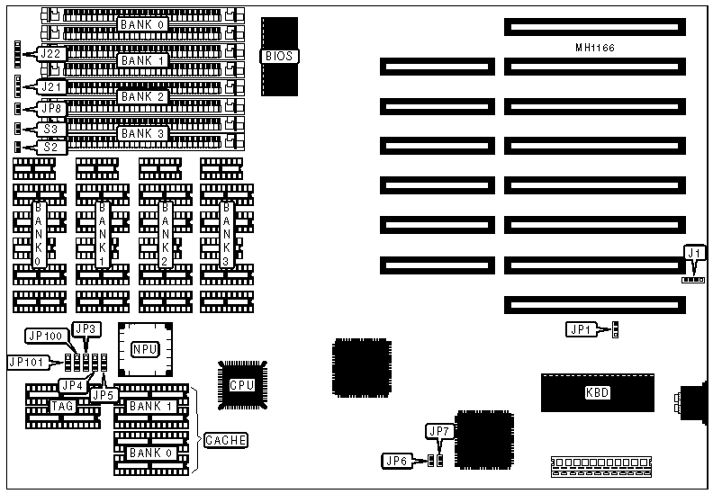
|
Processor |
80386SX |
|
Processor Speed |
20MHz |
|
Chip Set |
Unknown |
|
Max. Onboard DRAM |
16MB |
|
Cache |
32/64KB |
|
BIOS |
AMI |
|
Dimensions |
330.2mm x 218.4mm |
|
I/O Options |
None |
|
NPU Options |
80387SX |
|
CONNECTIONS | |||
|
Purpose |
Location |
Purpose |
Location |
|
External battery |
J1 |
Turbo LED |
JP8 |
|
Speaker |
J21 |
Reset switch |
S2 |
|
Power LED & keylock |
J22 |
Turbo switch |
S3 |
|
USER CONFIGURABLE SETTINGS | |||
|
Function |
Jumper |
Position | |
| » |
CMOS memory normal operation |
JP1 |
pins 2 & 3 closed |
|
CMOS memory clear |
JP1 |
pins 1 & 2 closed | |
|
DRAM (SIMM) CONFIGURATION | ||||
|
Size |
Bank 0 |
Bank 1 |
Bank 2 |
Bank 3 |
|
1MB |
(2) 256K x 9 |
(2) 256K x 9 |
NONE |
NONE |
|
2MB |
(2) 256K x 9 |
(2) 256K x 9 |
(2) 256K x 9 |
(2) 256K x 9 |
|
2MB |
(2) 1M x 9 |
NONE |
NONE |
NONE |
|
3MB |
(2) 256K x 9 |
(2) 256K x 9 |
(2) 1M x 9 |
NONE |
|
4MB |
(2) 1M x 9 |
(2) 1M x 9 |
NONE |
NONE |
|
5MB |
(2) 256K x 9 |
(2) 256K x 9 |
(2) 1M x 9 |
(2) 1M x 9 |
|
6MB |
(2) 1M x 9 |
(2) 1M x 9 |
(2) 1M x 9 |
NONE |
|
8MB |
(2) 1M x 9 |
(2) 1M x 9 |
(2) 1M x 9 |
(2) 1M x 9 |
|
9MB |
(2) 256K x 9 |
(2) 256K x 9 |
(2) 4M x 9 |
NONE |
|
10MB |
(2) 1M x 9 |
(2) 4M x 9 |
NONE |
NONE |
|
12MB |
(2) 1M x 9 |
(2) 1M x 9 |
(2) 4M x 9 |
NONE |
|
16MB |
(2) 4M x 9 |
(2) 4M x 9 |
NONE |
NONE |
|
DRAM (DIP) CONFIGURATION | ||||
|
Size |
Bank 0 |
Bank 1 |
Bank 2 |
Bank 3 |
|
1MB |
(4) 44256 and (2) 41256 |
NONE |
NONE |
NONE |
|
2MB |
(4) 44256 and (2) 41256 |
(4) 44256 and (2) 41256 |
NONE |
NONE |
|
3MB |
(4) 44256 and (2) 41256 |
(4) 44256 and (2) 41256 |
(4) 44256 and (2) 41256 |
NONE |
|
4MB |
(4) 44256 and (2) 41256 |
(4) 44256 and (2) 41256 |
(4) 44256 and (2) 41256 |
(4) 44256 and (2) 41256 |
|
SRAM JUMPER CONFIGURATION | |||||||
|
Size |
JP3 |
JP4 |
JP5 |
JP6 |
JP7 |
JP100 |
JP101 |
|
32KB |
pins 2 & 3 |
pins 1 & 2 |
pins 1 & 2 |
closed |
open |
pins 2 & 3 |
pins 1 & 2 |
|
64KB |
pins 2 & 3 |
pins 2 & 3 |
pins 2 & 3 |
open |
closed |
pins 2 & 3 |
pins 2 & 3 |
|
Note:Pins designated should be in the closed posiiton. | |||||||
|
SRAM CONFIGURATION | |||
|
Size |
Cache SRAM |
Location |
TAG |
|
32KB |
(4) 8K x 8 |
Banks 0 & 1 |
(2) 16K x 4 |
|
64KB |
(2) 32K x 8 |
Bank 0 |
(2) 16K x 4 |